Process and method for modifying polymer film surface interaction
a technology of surface interaction and polymer film, which is applied in the field of nano-printing, can solve the problems of reducing replication fidelity, damaging the template, and devastating the imprinting process, and achieves the effects of low surface energy, high replication fidelity, and easy industrial application
- Summary
- Abstract
- Description
- Claims
- Application Information
AI Technical Summary
Benefits of technology
Problems solved by technology
Method used
Image
Examples
example 1
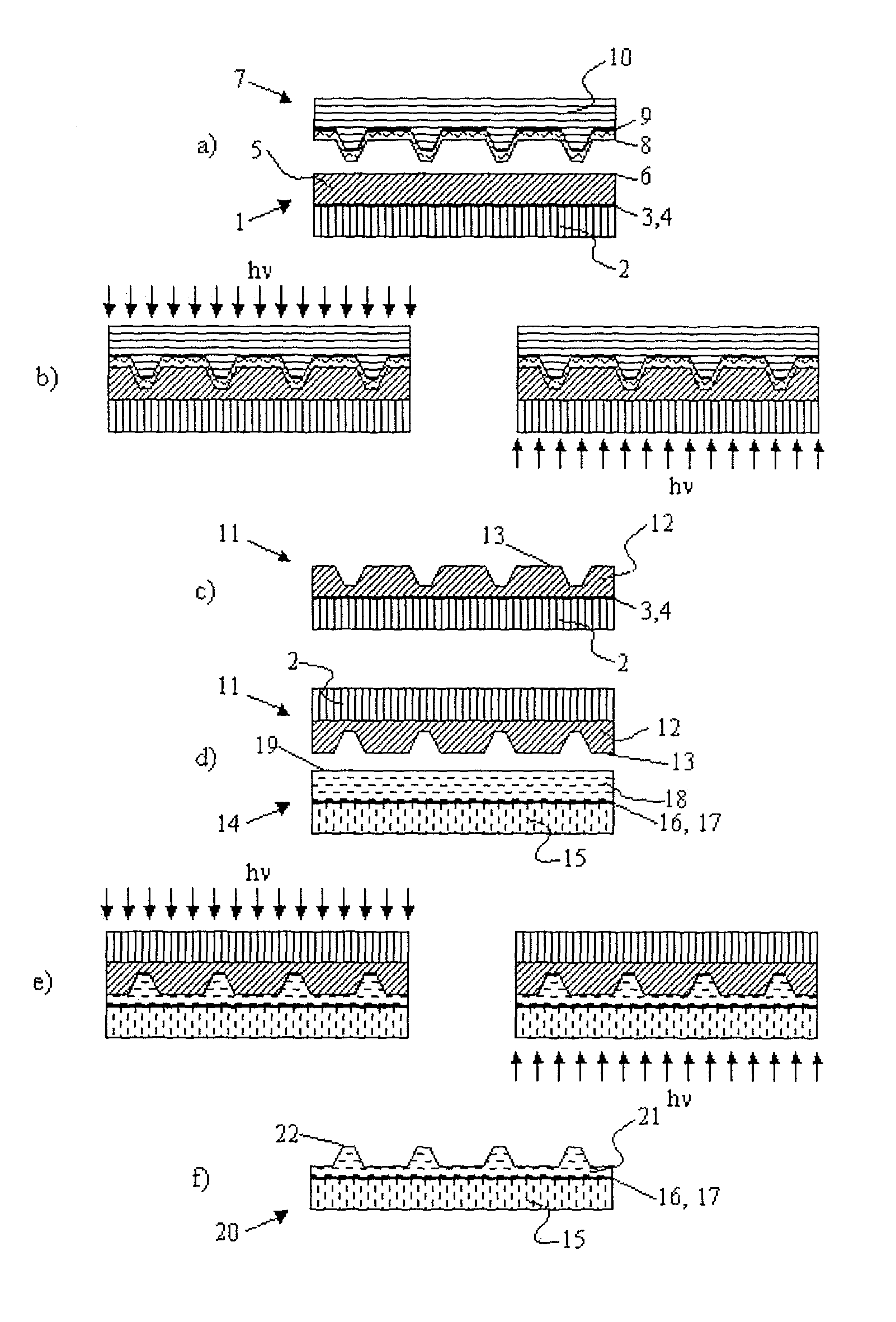
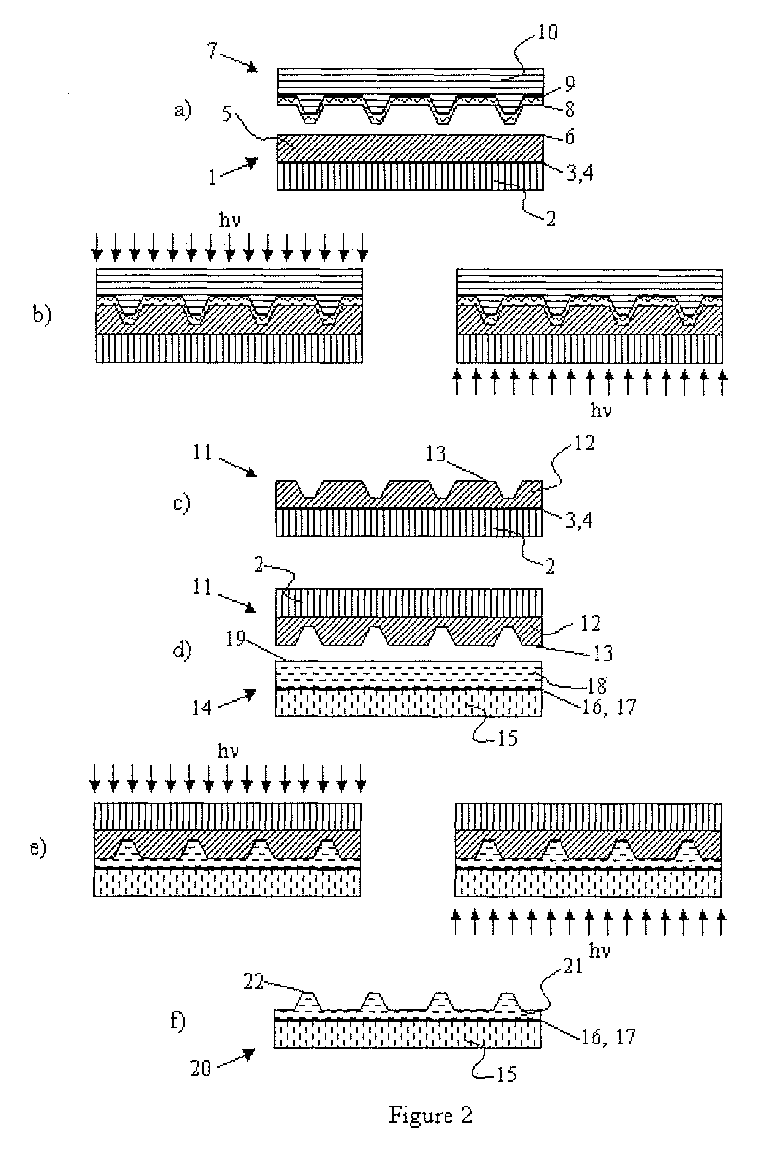
[0065]A 1.5 μm thick film of the IPS resists IPS70 / 95 was spin-coated onto a polycarbonate film having a thickness of 125 μm. A 2-step imprint process was carried out according to FIG. 2. The anti-sticking treated Ni stamp 1 was pressed against the polymer film for 60 sec with a pressure of 30 bars, the resist was cured with photon radiation for 90 sec as illustrated in FIG. 2b. During the exposure time the applied pressure was kept at 30 bars. Afterwards, the Ni stamp was separated from the cured IPS. The IPS comprising a polycarbonate film equipped with a completely cured IPS resist was applied in the second imprint process (FIG. 2d). A SR02 substrate resist was spin-coated to a thickness of 50 nm onto a silicon wafer, pretreated with an acrylate silane employed as an adhesion promoter for improved adhesion. The second imprint was performed as described above with a photon radiation time of 30 sec (FIG. 2e). After demolding, the cured substrate resist was examined by AFM. FIG. 3a ...
example 2
[0066]An imprint with Ni Stamp 2 was performed according to the description of Example 1 using a 1 μm thick SR20 / 47 film as substrate resist in the second imprint step and—in the second imprint step—with a photon radiation time of 60 sec. FIG. 3b displays an image of the substrate resist surface with dimensions of the applied Ni stamp pattern given in the caption of FIG. 3b.
example 3
[0067]An imprint with Ni Stamp 3 was performed according to the description of Example 1. However, the applied substrate resist (SR02) was 70 nm thick. FIG. 3c displays an image of the substrate resist surface with dimensions of the applied Ni stamp pattern given in the caption of FIG. 3c.
PUM
| Property | Measurement | Unit |
|---|---|---|
| contact angles | aaaaa | aaaaa |
| thickness | aaaaa | aaaaa |
| thickness | aaaaa | aaaaa |
Abstract
Description
Claims
Application Information


