Process and method for modifying polymer film surface interaction

a technology of surface interaction and polymer film, which is applied in the field of nano-printing, can solve the problems of reducing replication fidelity, damaging the template, and devastating the imprinting process, and achieves the effects of low surface energy, high replication fidelity, and easy industrial application

Active Publication Date: 2010-06-24
OBDUCAT AB SE
View PDF38 Cites 53 Cited by
  • Summary
  • Abstract
  • Description
  • Claims
  • Application Information

AI Technical Summary

Benefits of technology

[0010]It is an object of the invention to provide a material that comprising photo-reactive compounds with one or several types of chemical functionalities e.g. acrylates, epoxides or vinyl ethers. Additionally, the material comprises photo-initiators or catalysts and semi-fluorinated molecules. When contacting this material with a surface of a template, exhibiting low surface energy, the semi-fluorinated molecules will diffuse to the surface near region of that surface of the chemical composition facing the template surface. The material is coated on a polymer carrier object and used in an improved imprint process, having high replication fidelity, and which is easy and suitable to employ industrially.

Problems solved by technology

Any non-parallel arrangement or excessive pressure may therefore cause damage to the template.
Even though the dimensional change is small, it may be devastating in an imprint process, since the features of the pattern to be transferred are in the order of micrometers or even nanometers.
The result may therefore be reduced replication fidelity.

Method used


Image

  • Process and method for modifying polymer film surface interaction
  • Process and method for modifying polymer film surface interaction
  • Process and method for modifying polymer film surface interaction

Examples


example 1

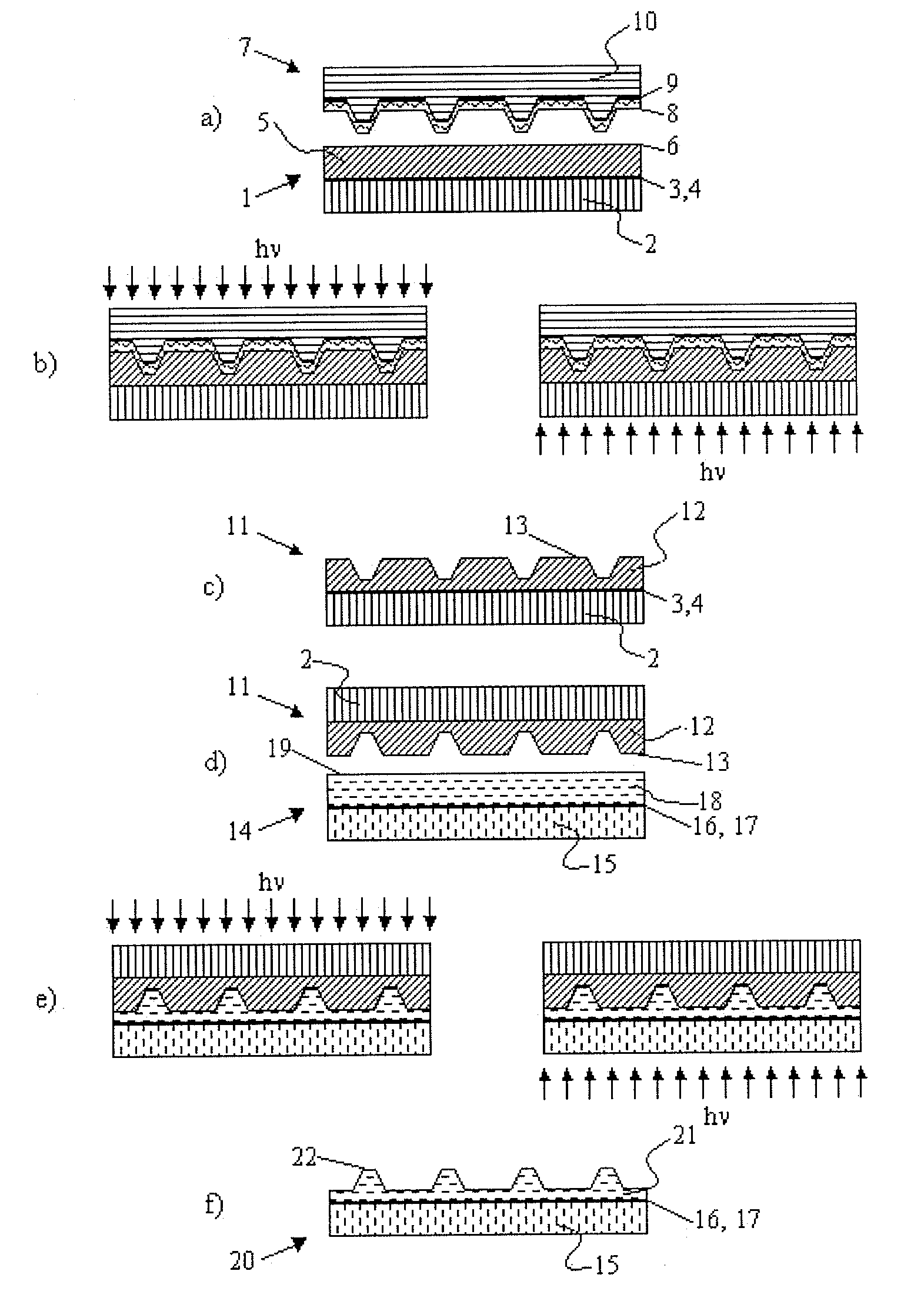
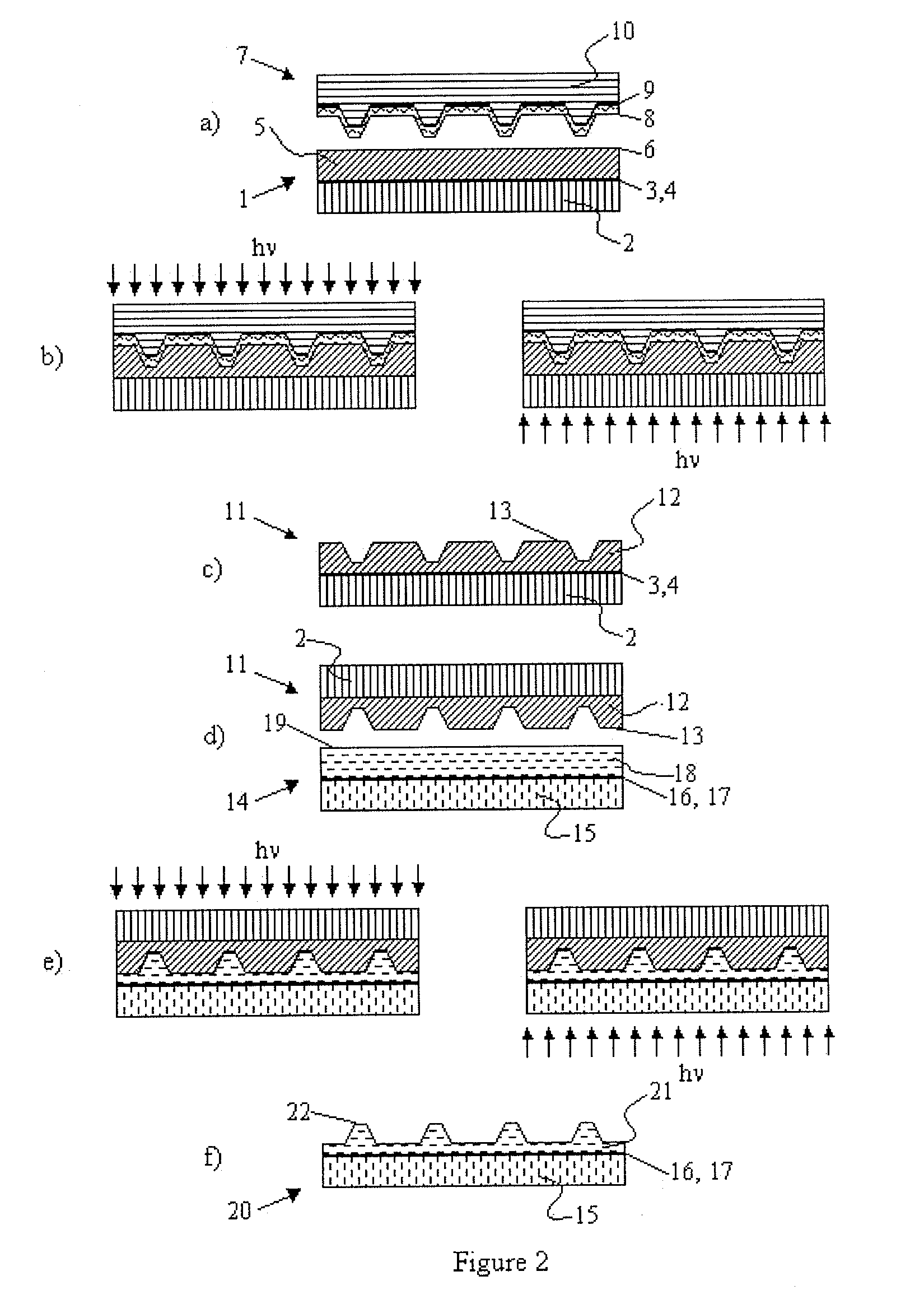
[0062]A 1.5 μm thick film of the IPS resists IPS70 / 95 was spin-coated onto a polycarbonate film having a thickness of 125 μm. A 2-step imprint process was carried out according to FIG. 2. The anti-sticking treated Ni stamp 1 was pressed against the polymer film for 60 sec with a pressure of 30 bars, the resist was cured with photon radiation for 90 sec as illustrated in FIG. 2b. During the exposure time the applied pressure was kept at 30 bars. Afterwards, the Ni stamp was separated from the cured IPS. The IPS comprising a polycarbonate film equipped with a completely cured IPS resist was applied in the second imprint process (FIG. 2d). A SR02 substrate resist was spin-coated to a thickness of 50 nm onto a silicon wafer, pretreated with an acrylate silane employed as an adhesion promoter for improved adhesion. The second imprint was performed as described above with a photon radiation time of 30 sec (FIG. 2e). After demolding, the cured substrate resist was examined by AFM. FIG. 3a ...

example 2

[0063]An imprint with Ni Stamp 2 was performed according to the description of Example 1 using a 1 μm thick SR20 / 47 film as substrate resist in the second imprint step and—in the second imprint step—with a photon radiation time of 60 sec. FIG. 3b displays an image of the substrate resist surface with dimensions of the applied Ni stamp pattern given in the caption of FIG. 3b.

example 3

[0064]An imprint with Ni Stamp 3 was performed according to the description of Example 1. However, the applied substrate resist (SR02) was 70 nm thick. FIG. 3c displays an image of the substrate resist surface with dimensions of the applied Ni stamp pattern given in the caption of FIG. 3c.


PUM

PropertyMeasurementUnit
surface energyaaaaaaaaaa
work of adhesionaaaaaaaaaa

Abstract

The invention provides a modification of a polymer film surface interaction properties. In this process a polymer carrier object is covered by a chemical composition, comprising photo-polymerizable compounds, photo-initiators or catalysts with the ability to initiate polymerization and semi-fluorinated molecules. The so-produced polymer mold contains semi-fluorinated moieties, which are predominantly located on the surface and on the surface near region of the patterned surface. The polymer mold is suitable as a template with modified properties in a nano-imprint lithography process.

Description

[0001]This application claims priority under 35 USC §119 (e) to U.S. Provisional Application No. 61 / 139,023 filed Dec. 19, 2008, and under 35 USC §119 (a) to European Application No. 08172338.9 filed on Dec. 19, 2008, the entire disclosures of which are incorporated herein by reference.TECHNICAL FIELD OF INVENTION[0002]The present invention relates to Nano-Imprinting in general and especially to the polymer mold with anti-sticking or anti-adhesion properties.BACKGROUND OF THE INVENTION[0003]One of the most powerful techniques for reproducing nanostructures—i.e. structures in the order of 100 nm or smaller—is nanoimprint lithography (NIL). In nanoimprint lithography an inverted copy of the surface pattern of a template—often called a stamp—is transferred into an object, comprising a substrate and, applied thereto, a film of a moldable layer often called resist, e.g. a polymer material. After heating the object to a temperature above the glass transition temperature of the polymer fil...

Claims


Application Information

Patent Timeline
Patent Type & Authority Applications(United States)
IPC IPC(8): B29C33/40B29C33/38
CPCB29C33/3857G03F7/0002B82Y40/00B82Y10/00Y10T428/3154Y10T428/31504B29C59/022
Inventor KEIL, MATTHIASNILSSON, JAKOBRING, JOHANHEIDARI, BABAK
Owner OBDUCAT AB SE
Why Eureka
Try Eureka