Semiconductor material doping based on target valence band discontinuity

a technology of valence band discontinuity and semiconductor materials, which is applied in the field of semiconductor device fabrication, can solve the problems of difficult control of doping during the manufacture of many types of devices fabricated with wide band gap semiconductor materials, and the conductivity of p-type algan is severely limited, and the effect of wide band gap gap gap

Active Publication Date: 2013-04-23
SENSOR ELECTRONICS TECH
View PDF5 Cites 28 Cited by
  • Summary
  • Abstract
  • Description
  • Claims
  • Application Information

AI Technical Summary

Problems solved by technology

Controlling doping during the manufacture of many types of devices fabricated with wide band gap semiconductor materials is difficult.
In particular, impurity levels for wide band gap semiconductor materials are deep and the activation of the impurities is inefficient, thereby making the doping more difficult to control.
As a result, the conductivity of p-type AlGaN is severely limited, which is extremely detrimental to the performance of deep ultraviolet light emitting diodes (LEDs).
However, as illustrated by FIG. 2, the conductance in a direction perpendicular to the two-dimensional hole gas is extremely small.

Method used


Image

  • Semiconductor material doping based on target valence band discontinuity
  • Semiconductor material doping based on target valence band discontinuity
  • Semiconductor material doping based on target valence band discontinuity

Examples


Embodiment Construction

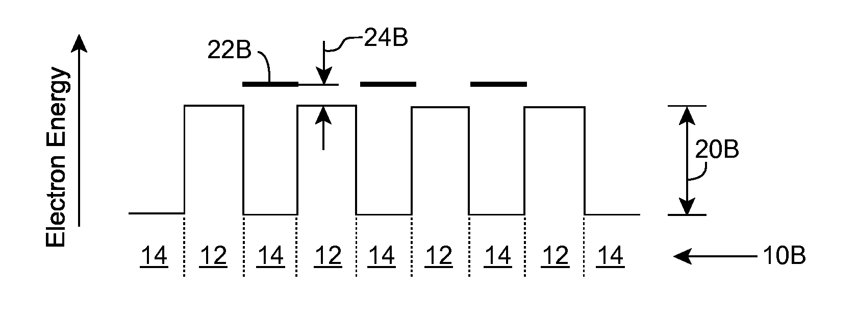
[0020]As indicated above, aspects of the invention provide a solution for designing and / or fabricating a structure including a quantum well and an adjacent barrier. A target band discontinuity between the quantum well and the adjacent barrier is selected to coincide with an activation energy of a dopant for the quantum well and / or barrier. For example, a target valence band discontinuity can be selected such that a dopant energy level of a dopant in the adjacent barrier coincides with a valence energy band edge for the quantum well and / or a ground state energy for free carriers in a valence energy band for the quantum well. The quantum well and the adjacent barrier can be formed such that the actual band discontinuity corresponds to the target band discontinuity. The resulting structure can provide a lower activation energy for the dopant in the barrier, which can result from a more efficient real space transfer of holes from the dopant (e.g., acceptor) energy level in the barrier i...


PUM


Abstract

A solution for designing and / or fabricating a structure including a quantum well and an adjacent barrier is provided. A target band discontinuity between the quantum well and the adjacent barrier is selected to coincide with an activation energy of a dopant for the quantum well and / or barrier. For example, a target valence band discontinuity can be selected such that a dopant energy level of a dopant in the adjacent barrier coincides with a valence energy band edge for the quantum well and / or a ground state energy for free carriers in a valence energy band for the quantum well. The quantum well and the adjacent barrier can be formed such that the actual band discontinuity corresponds to the target band discontinuity.

Description

REFERENCE TO PRIOR APPLICATIONS[0001]The current application claims the benefit of U.S. Provisional Application No. 61 / 266,523, titled “Method of Doping and Semiconductor Devices”, which was filed on 4 Dec. 2009, and which is hereby incorporated by reference.TECHNICAL FIELD[0002]The disclosure relates generally to semiconductor device fabrication, and more particularly, to the design and fabrication of a structure including a set of quantum wells and a set of barriers.BACKGROUND ART[0003]Controlling doping during the manufacture of many types of devices fabricated with wide band gap semiconductor materials is difficult. In particular, impurity levels for wide band gap semiconductor materials are deep and the activation of the impurities is inefficient, thereby making the doping more difficult to control. For example, FIG. 1 shows an illustrative fraction of activated impurities (Magnesium (Mg)) at 300 Kelvin (K) as a function of the impurity level in Aluminum Gallium Nitride (AlGaN)...

Claims


Application Information

Patent Timeline
Patent Type & Authority Patents(United States)
IPC IPC(8): H01L29/06H01L31/0336H01L31/0328H01L31/109H01L31/072
CPCB82Y10/00H01L29/122H01L29/2003H01L29/155H01L29/201H01L33/06H01L33/32
Inventor SHATALOV, MAXIM S.GASKA, REMIGIJUSYANG, JINWEISHUR, MICHAEL
Owner SENSOR ELECTRONICS TECH
Why Eureka
Try Eureka