Method for driving electro-optic device, electro-optic device, and electronic apparatus

a technology of electrooptic devices and electronic devices, applied in the direction of instruments, computing, electric digital data processing, etc., can solve the problems of image sticking, image sticking, image sticking, etc., to prevent image sticking, improve the performance of electronic devices, and improve display quality

Active Publication Date: 2013-05-07
JAPAN DISPLAY WEST
View PDF6 Cites 0 Cited by
  • Summary
  • Abstract
  • Description
  • Claims
  • Application Information

AI Technical Summary

Benefits of technology

[0008]An advantage of some aspects of the invention is that a method for driving an electro-optic device, an electro-optic device, and an electronic apparatus, which can suppress image sticking in a liquid crystal display device using the FFS mode, can be provided.

Problems solved by technology

A typical liquid crystal display device using the transverse electric field mode has a disadvantage in that electric charges tend to more easily remain compared with a liquid crystal display device using a twisted nematic (TN) mode in the related art because of the asymmetry in the electrode configuration, resulting in the occurrence of image sticking.
A liquid crystal display device using the FFS mode also has the disadvantage in that image sticking occurs, and a solution that can prevent the disadvantage is necessary.
However, the above-mentioned method in the related art has a problem.
Accordingly, when the method developed for a liquid crystal display device using the IPS mode is applied to a liquid crystal display device using the FFS mode, it is difficult to effectively suppress the accumulation of electric charges, and unfortunately, image sticking still occurs.
The accumulated electric charges may lead to a problem such as image sticking in the liquid crystal layer.

Method used


Image

  • Method for driving electro-optic device, electro-optic device, and electronic apparatus
  • Method for driving electro-optic device, electro-optic device, and electronic apparatus
  • Method for driving electro-optic device, electro-optic device, and electronic apparatus

Examples


Embodiment Construction

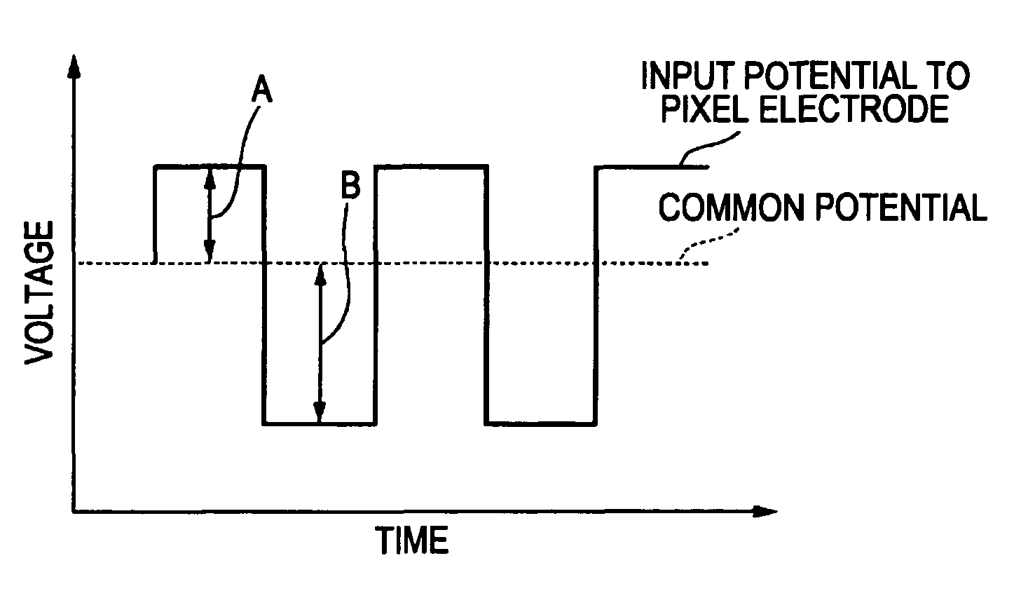
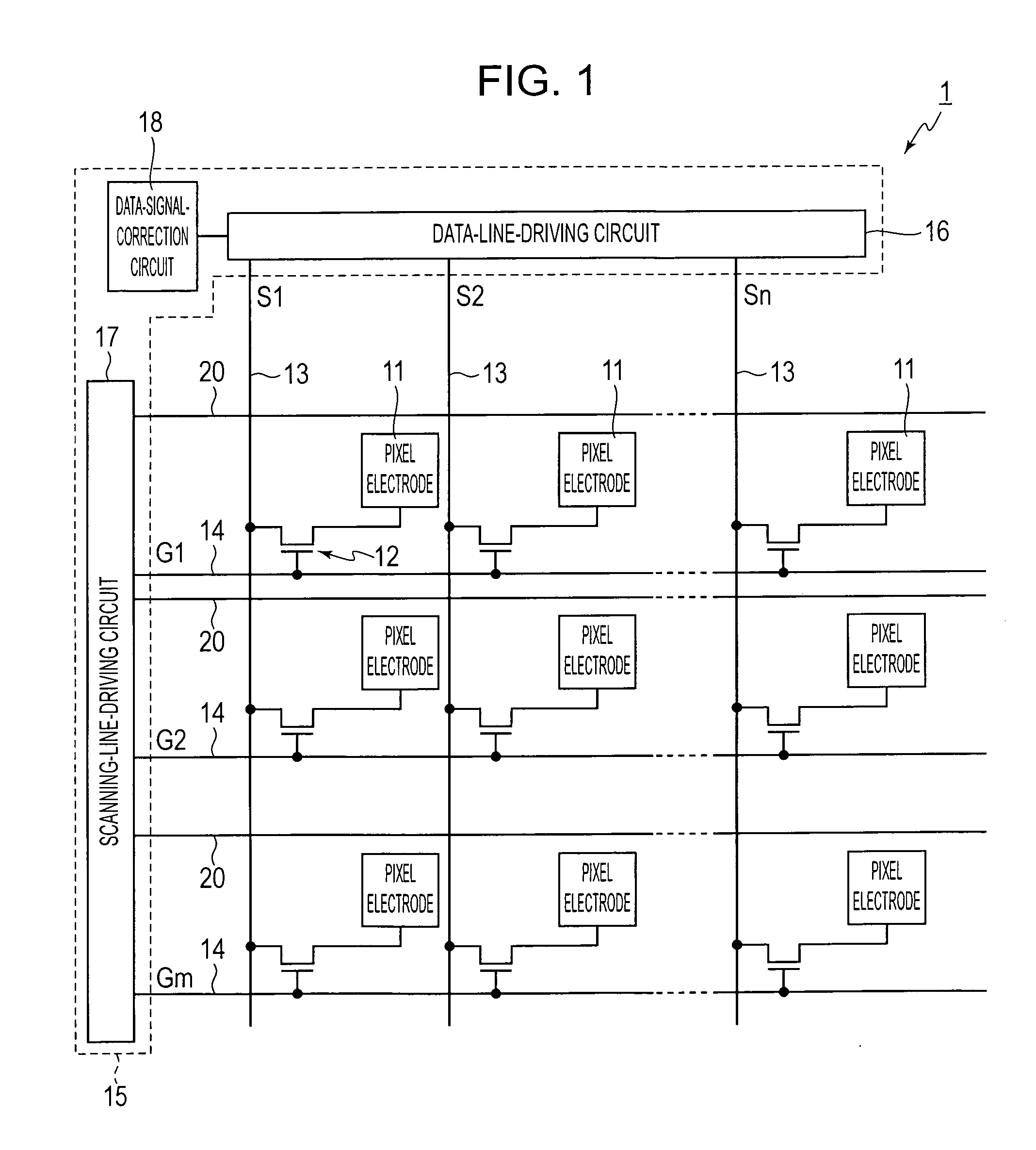
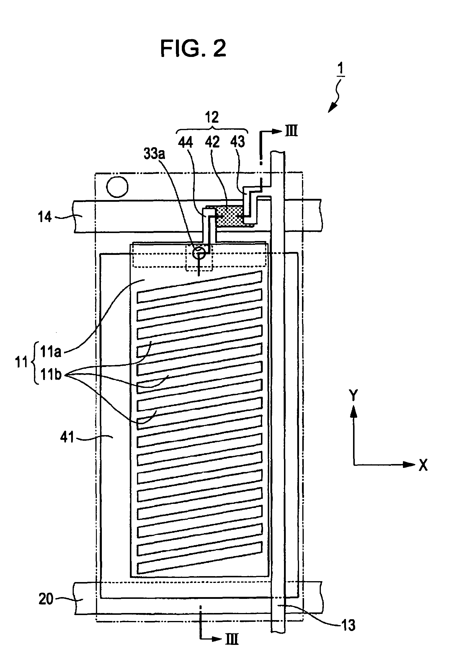
[0036]An embodiment of an electro-optic device according to the invention will be described with reference to the accompanying drawings. In the drawings used in the description below, the scale used for each element is appropriately varied so that the element is of a recognizable size. In the embodiment, a liquid crystal display device using the FFS mode is described as an example of the electro-optic device. FIG. 1 is a diagram showing an equivalent circuit of the liquid crystal display device. FIG. 2 is a partially enlarged structural plan view of a sub-pixel region of the liquid crystal display device. FIG. 3 is a cross-sectional view of the liquid crystal display device shown in FIG. 2, taken along the line III-III. FIG. 4 is a graph showing an optic-axis arrangement of the liquid crystal display device shown in FIG. 2.

Liquid Crystal Display Device

[0037]A liquid crystal display device 1 according to the embodiment of the invention is a color liquid crystal display device using t...


PUM


Abstract

A method for driving an electro-optic device includes a first and second electrode and a pair of substrates sandwiching an electro-optic layer driven by the first electrode. The method involves shifting one of two potentials input to at least one of the electrodes such that a potential difference between the first and second electrode where the potential input to the first electrode is higher than the potential input to the second electrode is larger than a potential difference between the first and second electrode where the potential input to the first electrode is lower than the potential input to the second electrode, when a gray-scale level where potential input to the first electrode is higher than potential input to the second electrode is equivalent to the gray-scale level where potential input to the first electrode is lower than potential input to the second electrode.

Description

CROSS-REFERENCE TO RELATED APPLICATION[0001]This application claims priority to Japanese Patent Application No. 2007-056933, filed in Japan on Mar. 7, 2007; the entire disclosure of which is expressly incorporated by reference.BACKGROUND[0002]1. Technical Field[0003]The present invention relates to a method for driving an electro-optic device, an electro-optic device, and an electronic apparatus.[0004]2. Related Art[0005]A mode in which the alignment of liquid crystal molecules is controlled in response to electric fields in the direction of a substrate that is generated across a liquid crystal layer (electro-optic layer) (hereinafter referred to as a “transverse electric field mode”) has been used to realize liquid crystal display devices (electro-optic devices) with a wide viewing angle. An in-plane switching (IPS) mode and a fringe-field switching (FFS) mode are known as such transverse electric field modes.[0006]A typical liquid crystal display device using the transverse electr...

Claims


Application Information

Patent Timeline
Patent Type & Authority Patents(United States)
IPC IPC(8): G09G3/36
CPCG09G3/3611G02F2001/134372G09G2300/0426G09G2300/0434G09G2310/06G02F1/134372
Inventor MURAI, HIDETOSHISEKIME, TOMOAKIKURASAWA, HAYATOOTA, JIN
Owner JAPAN DISPLAY WEST
Why Eureka
Try Eureka