Pixel structure

A pixel structure and pixel electrode technology, which is applied in nonlinear optics, instruments, optics, etc., can solve the problems of bad image retention and performance impact on the display screen, and achieve the effect of avoiding normal performance and suppressing image retention

Inactive Publication Date: 2010-06-09
CHUNGHWA PICTURE TUBES LTD
View PDF2 Cites 0 Cited by
  • Summary
  • Abstract
  • Description
  • Claims
  • Application Information

AI Technical Summary

Problems solved by technology

In this way, the performance of the second pixel electrode 119b will be affected by the residual charge, and then the next display screen will have a bad image sticking problem, so it is necessary to improve

Method used


Image

  • Pixel structure
  • Pixel structure
  • Pixel structure

Examples


no. 1 example

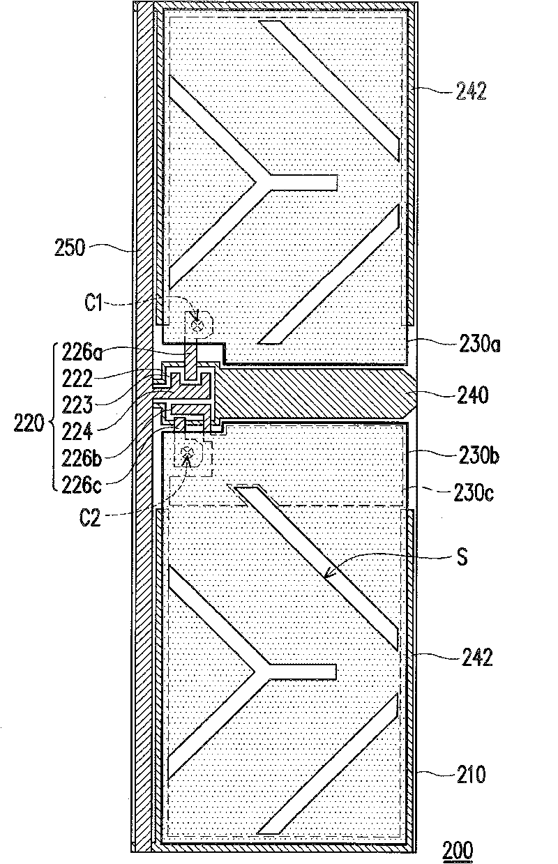
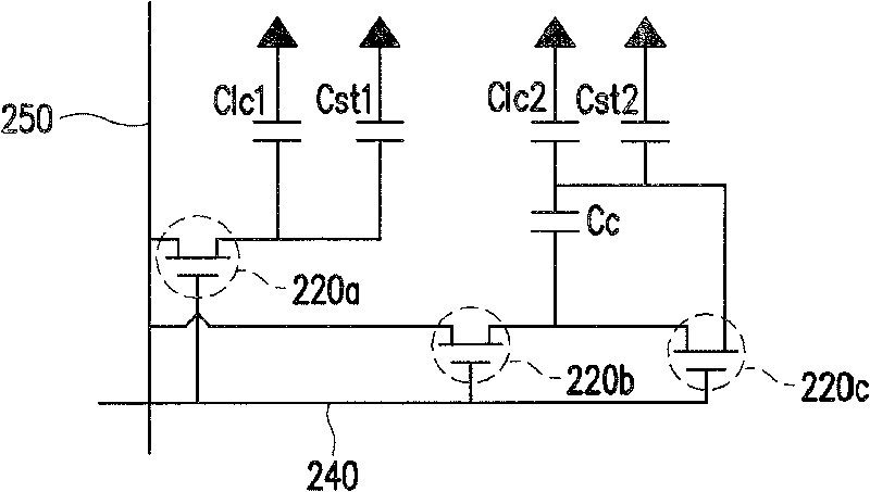
[0025] Figure 2A is a schematic diagram of the pixel structure of the first embodiment of the present invention, and Figure 2B is a schematic circuit diagram of the pixel structure of the first embodiment of the present invention. Please also refer to Figure 2A and Figure 2B , The pixel structure 200 of the present invention includes a thin film transistor 220 , a first pixel electrode 230 a , a second pixel electrode 230 b , a scan line 240 and a data line 250 . Wherein, the thin film transistor 220 is disposed on a substrate 210 and is electrically connected to the scan line 240 and the data line 250 . In actual production, the switch signal can be transmitted through the scanning line 240 to turn on the thin film transistor 220 , and the display signal can be transmitted to the first pixel electrode 230 a and the second pixel electrode 230 b through the data line 250 after the thin film transistor 220 is turned on.

[0026] In detail, the TFT 220 of the present inve...

no. 2 example

[0034] Figure 3A is a schematic diagram of the pixel structure of the second embodiment of the present invention, and Figure 3B is a circuit diagram of the pixel structure of the second embodiment of the present invention. Please also refer to Figure 3A and Figure 3B , The pixel structure 300 of the present invention includes a thin film transistor 320 , a first pixel electrode 330 a , a second pixel electrode 330 b , a scan line 340 and a data line 350 . Wherein, the thin film transistor 320 is disposed on a substrate 310 and is electrically connected to the scan line 340 and the data line 350 . In actual production, the switch signal can be transmitted through the scan line 340 to turn on the thin film transistor 320 , and the display signal can be transmitted to the first pixel electrode 330 a and the second pixel electrode 330 b through the data line 350 after the thin film transistor 320 is turned on.

[0035] In detail, the thin film transistor 320 of the present...


PUM


Abstract

The present invention discloses a pixel structure which comprises a grid electrode, a resource electrode, a first drain electrode, a second drain electrode, a third drain electrode, a first pixel electrode, a second pixel electrode, a scanning beam and a data wire; wherein, the grid electrode, the source electrode and the first electrode form a first film transistor; the grid electrode, the sourceelectrode and the second drain electrode form a second film transistor; the grid electrode, the second drain electrode and the third drain electrode form a sub-film transistor. Moreover, the first pixel electrode is connected with the first drain electrode, and the second drain electrode extends between the second pixel electrode and a base panel to form a capacitor coupling electrode. In addition, the second pixel electrode is connected with the third drain electrode of the sub-film transistor; the scanning beam is arranged on the base panel, and is connected with the grid electrode; the data wire is connected with the source electrode. The pixel structure of the present invention can effectively avoid the phenomenon of remaining images on a display picture. The pixel structure has favorable display quality.

Description

technical field [0001] The present invention relates to a pixel structure, and in particular to a pixel structure capable of improving display quality. Background technique [0002] The multimedia technology in today's society is quite developed, mostly benefiting from the progress of semiconductor components and display devices. As far as displays are concerned, liquid crystal displays with superior characteristics such as high image quality, good space utilization efficiency, low power consumption, and no radiation have gradually become the mainstream of the market. In order to improve the display quality of liquid crystal displays, various liquid crystal displays with wide viewing angles have been developed on the market, such as in-plane switching (IPS) liquid crystal displays and marginal field switching (IPS) liquid crystal displays. fringe field switching) liquid crystal display and multi-domain vertically aligned (multi-domain vertically aligned, MVA) liquid crystal...

Claims


Application Information

Patent Timeline
Patent Type & Authority Patents(China)
IPC IPC(8): G02F1/1362
Inventor 王明宗柳智忠张月泙戴孟杰
Owner CHUNGHWA PICTURE TUBES LTD
Why Eureka
Try Eureka