Liquid crystal display and method for producing the same

a liquid crystal display and liquid crystal technology, applied in the manufacture of electrode systems, electric discharge tubes/lamps, instruments, etc., can solve the problems of difficulty in realizing high luminance, and the pretilt conferred on the liquid crystal display device may not have adequate long-term reliability

Inactive Publication Date: 2014-03-25
MERCK PATENT GMBH
View PDF15 Cites 0 Cited by
  • Summary
  • Abstract
  • Description
  • Claims
  • Application Information

AI Technical Summary

Benefits of technology

[0045]According to the present invention, a liquid crystal display device whose image sticking is suppressed can be provided.

Problems solved by technology

Furthermore, in a VA-mode liquid crystal display device, the light transmittance in the regions in which slits, ribs, or rivets are provided is low, thus making it difficult to realize a high luminance.
However, a liquid crystal display device that has a pretilt conferred thereto may not have adequate long-term reliability.

Method used


Image

  • Liquid crystal display and method for producing the same
  • Liquid crystal display and method for producing the same
  • Liquid crystal display and method for producing the same

Examples


example 1

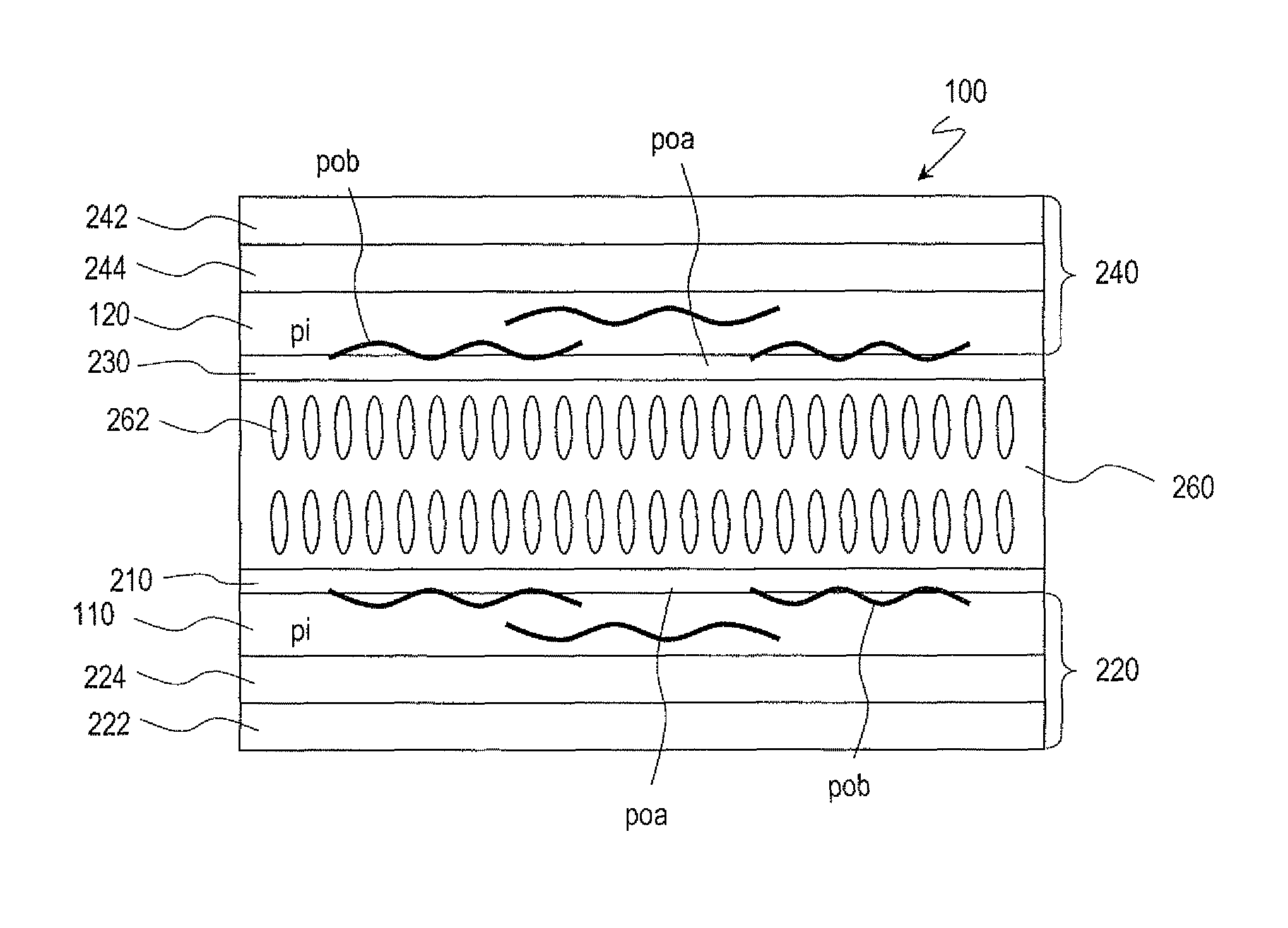
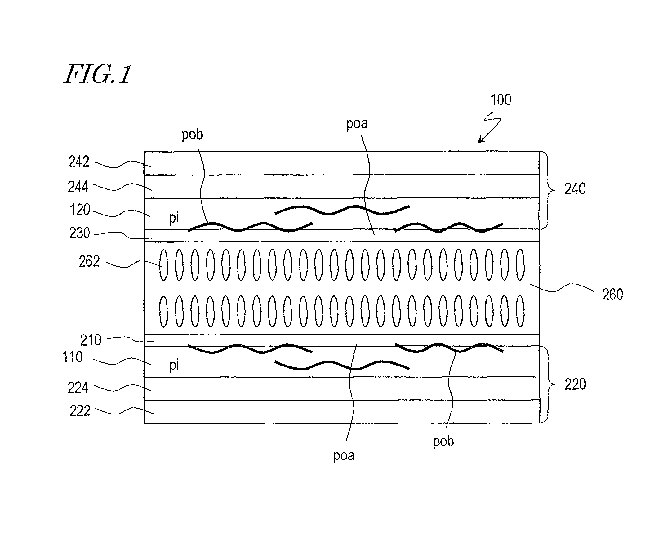
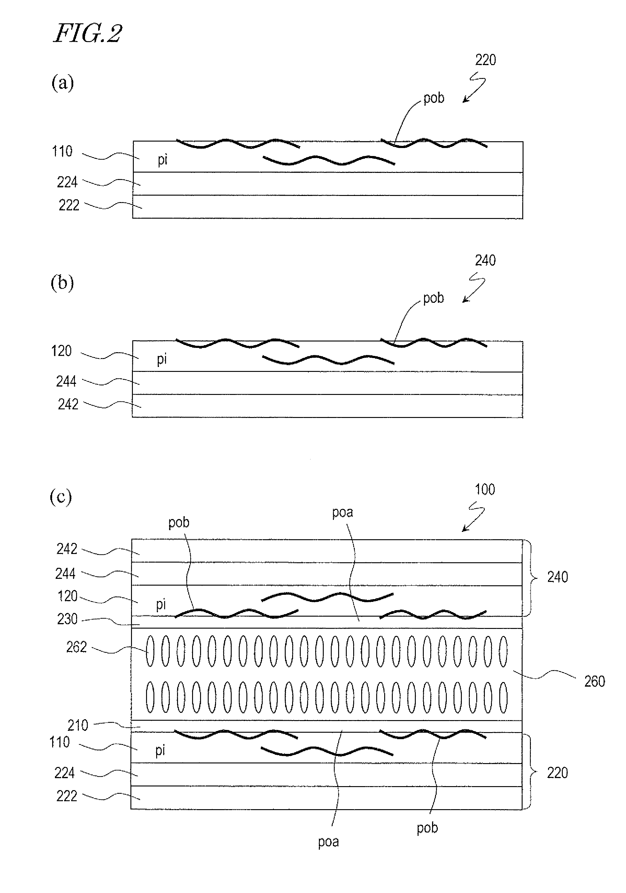
[0144]Hereinafter, with reference to FIG. 1, FIG. 6, and FIG. 8, a liquid crystal display device of Example 1 will be described. The liquid crystal display device of Example 1 also operates in the RTN mode.

[0145]First, on a principal face of the first insulative substrate 222, although not shown in the figures, TFTs and wiring lines connected to the TFTs, and an insulating layer and the like were formed, upon which the pixel electrodes 224 were formed. Similarly, on a principal face of the second insulative substrate 242, although not shown in the figures, a colored layer having color filters, and an insulating layer and the like were formed, upon which the counter electrode 244 was formed.

[0146]Next, an alignment film material was prepared. The alignment film material was obtained by allowing the precursor (polyamic acid) of the polyimide pi represented by structural formula (3a′) to be dissolved in a solvent, and thereafter allowing the polyfunctional monomer mb to be further diss...

example 2

[0160]Hereinafter, with reference to FIG. 1, FIG. 6, and FIG. 8, a liquid crystal display device of Example 2 will be described. The liquid crystal display device of Example 2 also operates in the RTN mode.

[0161]First, on a principal face of the first insulative substrate 222, although not shown in the figures, TFTs and wiring lines connected to the TFTs, and an insulating layer and the like were formed, upon which the pixel electrodes 224 were formed. Similarly, on a principal face of the second insulative substrate 242, although not shown in the figures, a colored layer having color filters, and an insulating layer and the like were formed, upon which the counter electrode 244 was formed.

[0162]Next, an alignment film material was prepared. The alignment film material was obtained by allowing a precursor (polyamic acid) of the polyimide pi to be dissolved in a solvent, and thereafter allowing the polyfunctional monomer mb and a cross-linker to be further dissolved therein. The prec...


PUM

PropertyMeasurementUnit
pretilt angleaaaaaaaaaa
wavelengthsaaaaaaaaaa

Abstract

A liquid crystal display device (100) according to the present invention includes: an active matrix substrate (220) having a pixel electrode (224); a counter substrate (240) having a counter electrode (244); a vertical-alignment type liquid crystal layer (260); and alignment sustaining layers (210, 230) provided between the active matrix substrate (220) and the liquid crystal layer (260) and between the counter substrate (240) and the liquid crystal layer (260). The alignment sustaining layers (210, 230) contain a polymerization product (poa) resulting from polymerization of a polyfunctional monomer. At least one of the active matrix substrate and the counter substrate further includes an alignment film (110, 120) located on the liquid crystal layer side, the alignment film (110, 120) containing polyimide (pi) and a polymerization product (pob) resulting from polymerization of a polyfunctional monomer.

Description

[0001]This application is the U.S. national phase of International Application No. PCT / JP2009 / 002931, filed 25 Jun. 2009, which designated the U.S. and claims priority to JP Application No. 2008-303176, filed 27 Nov. 2008, the entire contents of each of which are hereby incorporated by reference.TECHNICAL FIELD[0002]The present invention relates to a liquid crystal display device and a method of producing the same.BACKGROUND ART[0003]Liquid crystal display devices are used not only as small-sized display devices, e.g., the display sections of mobile phones, but also as large-sized television sets. Liquid crystal display devices of the TN (Twisted Nematic) mode, which have often been used conventionally, have relatively narrow viewing angles. In recent years, however, liquid crystal display devices with wide viewing angles have been produced, e.g., the IPS (In-Plane Switching) mode and the VA (Vertical Alignment) mode. Among such modes with wide viewing angles, the VA mode is adopted...

Claims


Application Information

Patent Timeline
Patent Type & Authority Patents(United States)
IPC IPC(8): G02F1/1337
CPCG02F1/133723G02F2001/133397C08G73/12G02F1/133753G02F2001/133715G02F1/133788C08G73/1078G02F2001/133742C08L79/085C08L79/08Y10T428/1005Y10T428/1023C09K2323/02C09K2323/027G02F1/133397G02F1/133715G02F1/133742
Inventor MIZUSAKI, MASANOBUNAKANISHI, YOHEI
Owner MERCK PATENT GMBH
Why Eureka
Try Eureka