Light emitting device

a technology of light-emitting devices and led chips, which is applied in the direction of solid-state devices, semiconductor devices, printed circuit aspects, etc., can solve the problems of difficult to adequately transfer heat from led chips (dies) through the package, significant change in the correlated color temperature (cct) and/or luminous flux of light emitted by the device, and high manufacturing cost, so as to maximize heat dissipation, minimize the thermal resistance of the package, and high a thermal conductivity

Active Publication Date: 2013-05-14
EPISTAR CORP
View PDF22 Cites 12 Cited by
  • Summary
  • Abstract
  • Description
  • Claims
  • Application Information

AI Technical Summary

Benefits of technology

[0013]In order for the device to generate a desired color of light or white light with a selected correlated color temperature (CCT), each recess can be at least partially filled with a mixture of at least one phosphor material and a light transmissive material. The at least one phosphor material is configured to absorb at least a portion of the light emitted by the LED chips and to emit light having a dominant wavelength in a second wavelength range. Typically, the emission product of the device appears white in color and comprises a combination of light of the first and second wavelength ranges. Alternatively, the emission product of the device can comprise light generated by the at least one phosphor material. Providing a respective recess for each LED chip provides the benefit of reducing the quantity of phosphor material required as compared with known packages in which a single recess is used to house an array of LED chips. Moreover, it has been found that such a package has an improved brightness compared to the known packages. Typically, the cover is essentially planar and the recesses can conveniently be filled by sweeping (drawing) the phosphor / polymer mixture over the surface of the cavity cover using a flexible blade such as doctor blade, squeegee or alike. A benefit of such a method is that it eliminates the need to dispense a measured quantity of phosphors into each recess and thereby reduces costs.
[0015]To minimize the thermal resistance of the package and to maximize dissipation of heat, the substrate has as high a thermal conductivity as possible and is preferably of order of at least 200 Wm−1 K−1. The substrate is preferably a metal advantageously copper or a copper alloy, though it can comprise other metals or alloys such as aluminum, an aluminum alloy, a magnesium alloy or a thermally conducting ceramic such as aluminum silicon carbide (AlSiC) or a carbon composite.
[0016]Advantageously the cover is also made of a material that is a good thermal conductor and has a thermal conductivity of at least 150 Wm−1 K−1 and preferably at least 200 Wm−1 K−1. Such a cover can provide heat sinking of the phosphor material and reduce potential thermal degradation of the phosphor material. The cover preferably comprises a metal, advantageously copper or a copper alloy, though it can comprise other metals or alloys such as aluminum, an aluminum alloy, a magnesium alloy or a thermally conducting ceramic such as aluminum silicon carbide (AlSiC) or a carbon composite.
[0017]In one arrangement intended for LED chips having a “lateral” conducting structure in which both LED electrodes are located on the same face, typically the light emitting surface of a surface emitting LED, the device further comprises an electrical circuit arrangement mounted on the substrate which has a plurality of through-holes configured such that each chip is directly mounted to the substrate. In this specification “directly mounted” means mounted in direct thermal communication without intervening layer(s) and includes soldering the chips to the substrate. Each LED chip is electrically connected to the circuit arrangement using for example bond wires. The circuit arrangement preferably comprises a printed circuit board (PCB) such as an FR-4 PCB. A particular advantage of this packaging arrangement is that each LED chip is mounted in direct thermal communication with a high thermal conductivity substrate and this provides a very low thermal resistance and improved heat sinking of the chips compared with the known solutions. Additionally, the use of a circuit layer overlying the chips to provide electrical connection of the LED chips ensures complete electrical isolation from the substrate. This is beneficial for devices intended for use in general lighting, which are often required to operate from high voltage alternating current supplies of 110V or 220V.

Problems solved by technology

A problem with such existing light emitting devices, in particular white light emitting devices intended for general lighting which typically require an emitted luminous flux of 500 lumens or greater (i.e. an input power of typically 5 W to 10 W), is thermal management and in particular adequately dissipating heat generated by such devices.
A further problem is thermal degradation of the phosphor material with time which can result in a significant change in the correlated color temperature (CCT) and / or luminous flux of light emitted by the device.
However, the thermal resistance of the package can make it difficult to adequately transfer heat from the LED chips (dies) through the package which is often fabricated from an electrically insulating material such as a high temperature polymer or ceramic.
Whilst such a device package performs well both electrically and thermally (i.e. thermal resistance is typically 8 to 10° C. / W), such packages are relatively expensive to fabricate which can limit the applications for which they are cost effective.
Whilst the thermal resistance of an MCPCB is excellent and can be as low as 1.5° C. / W the cost of such a packaging arrangements, in particular the cost of applying phosphor material to individual LED chips, can be prohibitively expensive in the highly competitive cost conscious general lighting sector.
Moreover with such a packaging arrangement it can be difficult to produce devices with a consistent CCT.
Moreover, it is believed that thermal degradation of the phosphor material maybe higher in a device where a single recess housing multiple LED chips.

Method used


Image

  • Light emitting device
  • Light emitting device
  • Light emitting device

Examples


first embodiment

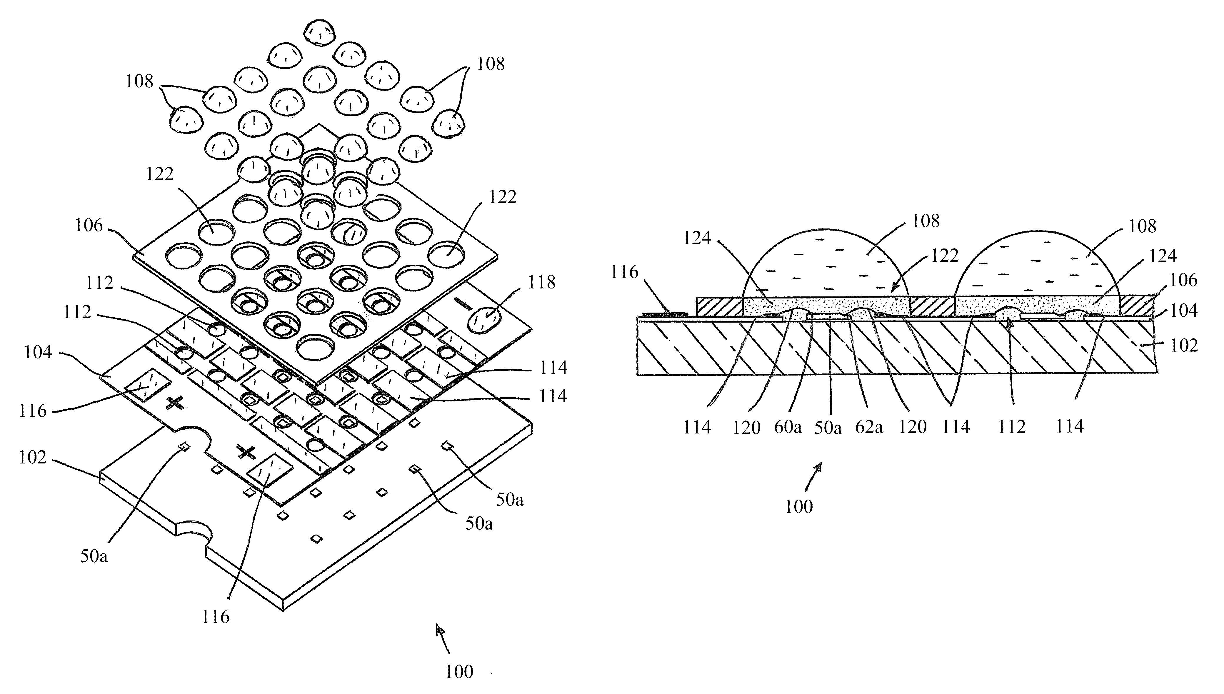
[0040]A light emitting device 100 in accordance with the invention will now be described with reference to FIGS. 3, 4 and 5 in which FIG. 3 is a perspective view of the device, FIG. 4 is an exploded perspective view showing the device's construction and FIG. 5 is a schematic sectional view through a line A-A of FIG. 3. For ease of understanding no phosphor material is shown in FIGS. 3 and 4. The device 100 is configured to generate white light of a selected CCT (for example 5500K) and a luminous flux of order 600 lumens (approximately 12 W input power).

[0041]The device 100 is of a layered (laminated) construction and comprises three layers: a thermally conductive base (substrate) 102, a circuit layer 104, a cavity cover 106 and an array of lenses 108 (N.B. the lenses 108 are omitted in FIG. 3). The device further comprises twenty four 500 mW blue (i.e. dominant wavelength in a range ≈400 to ≈480 nm) surface emitting “lateral” conducting InGaN / GaN (indium gallium nitride / gallium nitr...

second embodiment

[0054]A light emitting device 100 in accordance with the invention will now be described with reference to FIGS. 7, 8 and 9 in which FIG. 7 is a perspective view of the device, FIG. 8 is an exploded perspective view showing the device's construction and FIG. 9 is a schematic sectional view through a line A-A of FIG. 7. The device 100 is configured to generate white light of a selected CCT and a luminous flux of order 1000 lumens (approximately 21 W input power).

[0055]In common with the device described above the device 100 comprises three layers: a thermally conductive base 102, a circuit layer 104, a cavity cover 106 and an array of lenses 108. The base 102 comprises a material with as high a thermal conductivity as possible (typically of the order of at least 200 Wm−1 K−1) such as a metal and is preferably made of copper. In this embodiment the circuit layer 104 comprises an electrically insulating, thermally conductive film 126 deposited on the base 102 on which a pattern of elec...


PUM


Abstract

A light emitting device comprises a plurality of LED chips (“lateral” or “vertical” conducting) operable to generate light of a first wavelength range and a package for housing the chips. The package comprises: a thermally conducting substrate (copper) on which the LED chips are mounted and a cover having a plurality of through-holes in which each hole corresponds to a respective one of the LED chips. The holes are configured such that when the cover is mounted to the substrate each hole in conjunction with the substrate defines a recess in which a respective chip is housed. Each recess is at least partially filled with a mixture of at least one phosphor material and a transparent material. In a device with “lateral” conducting LED chips a PCB is mounted on the substrate and includes a plurality of through-holes which are configured such that each chip is directly mounted to the substrate. For a device with “vertical” conducting LED chips the LED chips are mounted on a diamond like carbon film.

Description

CROSS-REFERENCE TO RELATED APPLICATIONS[0001]This application claims the benefit of priority of U.S. Provisional Application No. 61 / 180,065, filed May 20, 2009 and entitled “Light Emitting Device” by Hwa S U et al., the contents of which are incorporated herein by reference.BACKGROUND OF THE INVENTION[0002]1. Field of the Invention[0003]This invention relates to light emitting devices and more especially to packaging arrangements for such devices. In particular, although not exclusively, the invention relates to light emitting devices which include one or more phosphor (photo-luminescent) materials to generate a desired emission product color. Moreover embodiments of the invention concern, but are not limited to, white light generating devices for general lighting applications with a high emission intensity (i.e. a luminous flux of more than 500 lumens) that are based on light emitting diodes (LEDs).[0004]2. Description of the Related Art[0005]White light emitting LEDs (“white LEDs”...

Claims


Application Information

Patent Timeline
Patent Type & Authority Patents(United States)
IPC IPC(8): H01L51/40H01L21/00
CPCH01L25/0753H05K1/021H01L2224/49107H01L33/58H01L33/64H01L33/647H01L2224/32225H01L2224/48091H01L2224/48227H01L2224/73265H01L2924/01004H01L2924/01012H01L2924/0102H01L2924/01025H01L2924/01057H01L2924/01063H01L2924/01079H01L2924/09701H05K2201/10106H01L33/50H01L2924/01322H01L2924/01087H01L2924/01068H01L2924/01067H01L2924/01066H01L2924/01019H01L2924/00014H01L2924/00
Inventor SU, HWACHOU, HSI-YANHUANG, CHIH WEI
Owner EPISTAR CORP
Why Eureka
Try Eureka