High resolution magnetic read head using top exchange biasing and/or lateral hand biasing of the free layer

a magnetic read head and free layer technology, applied in the field of mr sensor fabrication, can solve the problems of less effective orientation of free layer magnetization, adversely affecting snr, and more thermal noise, and achieve the effect of improving down-track linear resolution

Active Publication Date: 2013-05-28
HEADWAY TECH INC
View PDF9 Cites 21 Cited by
  • Summary
  • Abstract
  • Description
  • Claims
  • Application Information

AI Technical Summary

Benefits of technology

[0014]A first object of this invention is to provide a MR read head design with improved down-track linear resolution without the necessity of a narrower read gap.
[0015]A second object of the present invention is to provide such a read head design by the use of a synthetic-antiferromagnetic (SAF) free layer (FL) structure, for achieving a high linear resolution without the use of read shields to shunt away interference from adjacent data bits during the read-back process.
[0030]Note that depending upon the positioning of the HB layers relative to the layers (21) and (22), the HB field in these layers can be different from each other. In the configuration of FIG. 2(A), the fields differ by little more than 5%. However, in embodiments nine through sixteen to be described below, variations in the HB field can be tuned by changing the thickness of the layer and its position relative to layer (21). For example, a particularly good sensor performance was found when the top surface of layer (5) was aligned with the top surface of layer (21), while still allowing a smaller, (approximately 20%) HB field at the center of layer (22). In simulations with (a) X+Y greater than or equal to 100, meaning the bias field on layer (21) is slightly stronger than that on (22) in the opposite direction and (b) with X<Y, meaning that the field from the HB layer on (21) is stronger than that on (22), we can obtain better down-track performance. In case (b), we can make HB layer (5) thinner, so that X<Y.
[0033]The biasing scheme described above, with X+Y=100, produces a symmetric magnetic response in the two magnetic layers in the SAF free layer. This results in the best down-track resolution and signal stability, which is an object of the invention.

Problems solved by technology

The fewer the magnetic charges, the less is the pinning field of the HB layers and the less effective they are at orienting the free layer magnetization.
This, in turn, allows more thermal noise as a result of domain perturbations and a poorer SNR.
Poorer pinning, in turn, will ultimately also adversely affect SNR.
Thus, improving resolution by reducing the RG thickness of the sensor is not practical.

Method used


Image

  • High resolution magnetic read head using top exchange biasing and/or lateral hand biasing of the free layer
  • High resolution magnetic read head using top exchange biasing and/or lateral hand biasing of the free layer
  • High resolution magnetic read head using top exchange biasing and/or lateral hand biasing of the free layer

Examples


embodiment 1

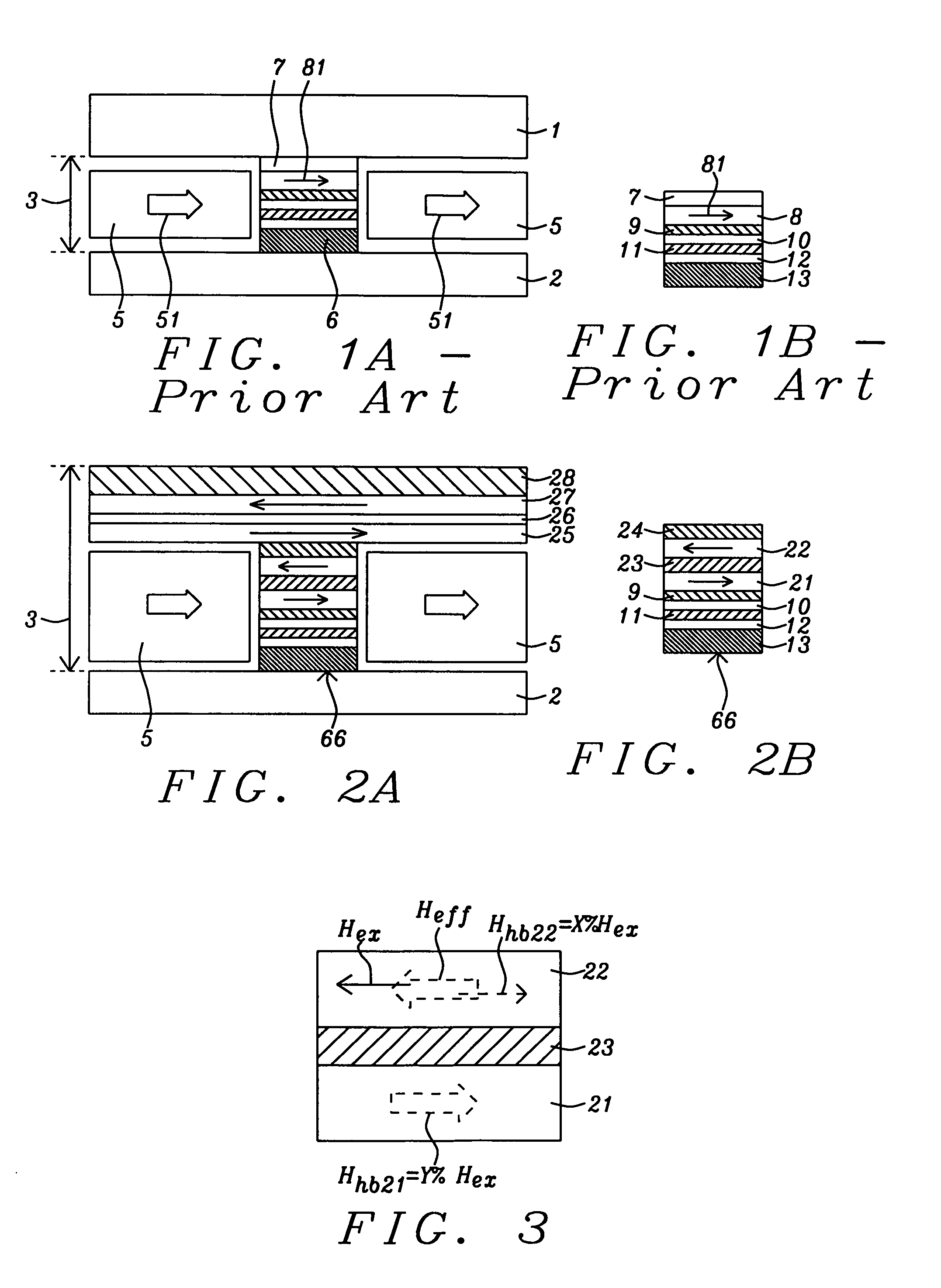
[0066]The first embodiment of the present invention has already been described above with reference to FIG. 2(A) and FIG. 2(B). Remaining embodiments 2 through 16 are described below with reference to FIG. 6 through FIG. 20 respectively. It is understood that the discussion of the effects of the top exchange biasing structure and the side hard biasing layers will apply equally well to the remaining embodiments described below. It is also understood that the processes by which each of the embodiments are formed are substantially identical, specifically with respect to the sequence of anneals in which AFM pinning (13) and pinned layers in the stack are annealed first at a high temperature and field and the top AFM pinning layer (28) of the top biasing structure is annealed last at a lower temperature and smaller field so as not to affect the first annealing results of layer (13). The HB layer is provided with its own anneal, substantially similar to the weaker field anneal of the top ...

embodiment 2

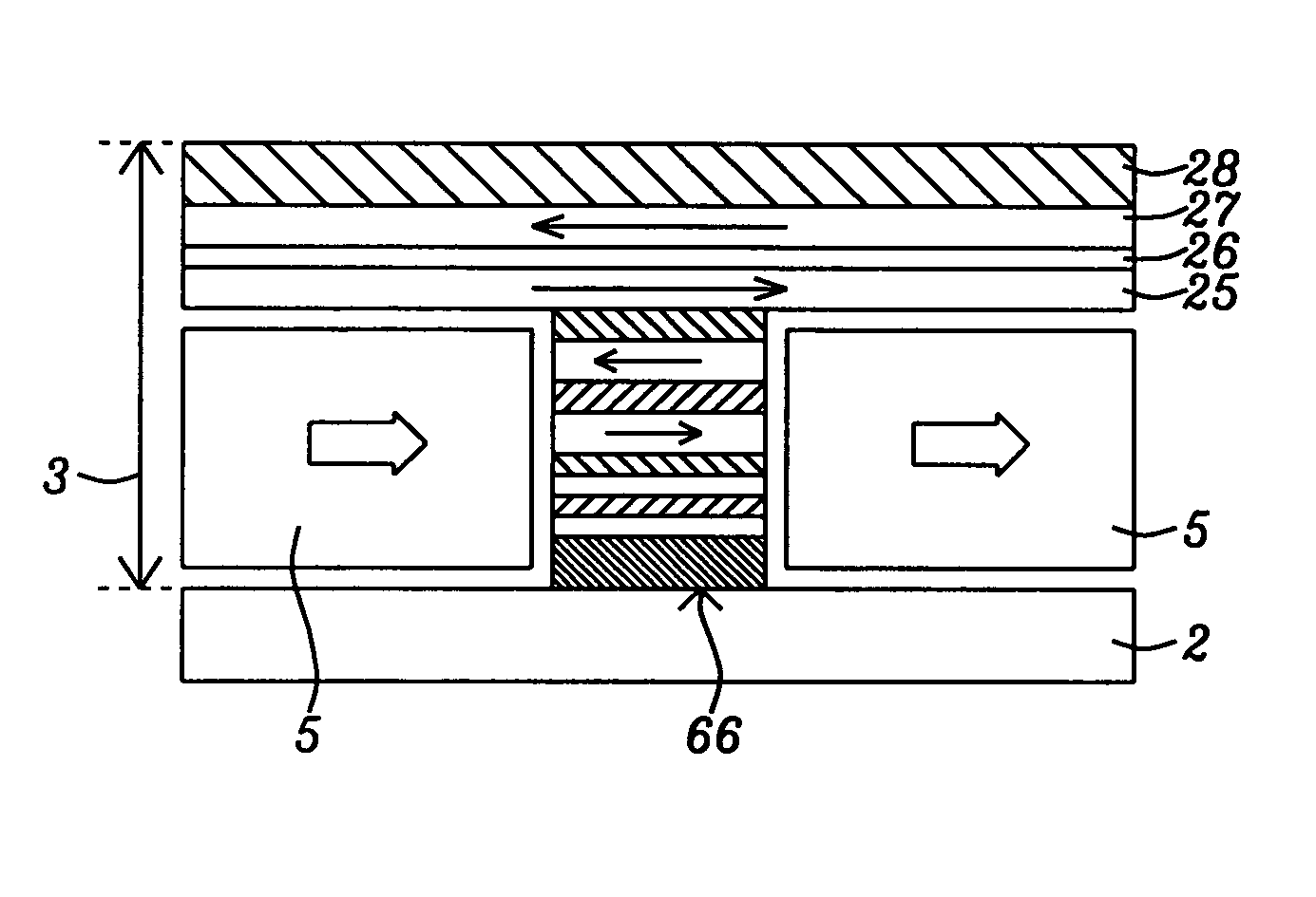
[0070]Referring now to FIG. 6, there is shown schematically a second embodiment of the present invention which is in all other aspects the same as the first embodiment illustrated schematically in FIG. 2(A) and FIG. 2(B) and described above, except that the top biasing structure, (28) and (25), that provides the exchange bias by exchange coupling to the free layer element (22) across coupling layer (24), includes only a single magnetic layer, layer (25), that is itself exchange coupled to an AFM pinning layer (28). The pinning direction of layer (28) on layer (25), is from left to right as shown by arrow (251). The formation of this embodiment, in annealing steps and patterning steps, is in all respects the same as described for embodiment 1 with the sole exception being the deposition of single layer (25) rather than the tri-layer of (25), (26) and (27) in the first embodiment.

embodiment 3

[0071]Referring now to FIG. 7, there is shown schematically a third embodiment of the present invention that is similar in all other aspects to the first embodiment, except that the MR stack, indicated as (67) (unlike stack (66) in FIG. 6) is not patterned horizontally (reduced in its width by etching) all the way down to AFM pinning layer (13) as in FIG. 2(A). Thus, the MR stack (67) of this embodiment has a uniformly narrow width encompassing the vertically stacked horizontal layers (24), (22), (23), (21) and (9), but is not horizontally patterned through layers (10), (11), (12) and (13), which retain a wider width. Subsequent to patterning, the hard biasing layers (5) are formed over the laterally extending unpatterned layers (10), (11), (12) and (13), with necessary isolation and seed layers (not indicated) between (5) and (10). Thus, the biasing layers (5) are now highly symmetrically placed relative to the SAF free layer structure and can provide similar fields to the two magn...


PUM

PropertyMeasurementUnit
thicknessaaaaaaaaaa
thicknessaaaaaaaaaa
thicknessaaaaaaaaaa

Abstract

A CPP (Current Perpendicular to Plane) MR (Magnetoresistive) read head and its method of fabrication includes a patterned CPP MR sensor stack having a SAF (Synthetic Antiferromagnetic) free layer structure that is longitudinally biased by the combination of an exchange biasing layer formed over the sensor stack and hard biasing layers that are formed adjacent to the patterned sides of the stack. The combination provides the stack with high resolution reading capabilities without the necessity for a narrow read gap formed by closely spaced top and bottom shields. Sixteen embodiments are described that provide different versions of the exchange biasing layer, different positions of the hard biasing layers and different patternings of the CPP MR sensor stack.

Description

BACKGROUND OF THE INVENTION[0001]1. Field of the Invention[0002]This invention relates generally to the fabrication of a MR sensor, which can be a tunneling magnetoresistive (TMR) sensor or a giant magnetoresistive (GMR) sensor. In particular it relates to an MR sensor in which resolution is increased by use of a synthetic antiferromagnetic (SAF) free layer structure.[0003]2. Description of the Related Art[0004]With the ever increasing areal density with which data is stored on magnetic media such as disks in hard disk drives (HDD), the magnetoresistive (MR) sensor that is used as the read-back element in the HDD is required to have a correspondingly improved spatial resolution while achieving and maintaining a reasonable signal-to-noise ratio (SNR). Referring to schematic FIGS. 1a, and 1b, there are shown two views of a generic, prior-art current-perpendicular-to-plane (CPP) tunneling magnetoresistive (TMR) read head.[0005]FIG. 1(A) illustrates the read head in a vertical cross-sec...

Claims


Application Information

Patent Timeline
Patent Type & Authority Patents(United States)
IPC IPC(8): G11B5/39
CPCG01R33/098G11B5/3932Y10T29/49048Y10T29/49044G11B5/3909G11B2005/3996
Inventor ZHOU, YUCHENCHEN, WENYUSMYTH, JOE
Owner HEADWAY TECH INC
Why Eureka
Try Eureka