Supercharge Your Innovation With Domain-Expert AI Agents!

Lead frame assembly, package structure and LED package structure

a technology of led frame and assembly, which is applied in the direction of semiconductor devices, semiconductor/solid-state device details, electrical devices, etc., can solve the problems of troublesome manufacturing process and high manufacturing cos

Active Publication Date: 2013-06-04
LITE ON TECH CORP +1
View PDF16 Cites 0 Cited by
  • Summary
  • Abstract
  • Description
  • Claims
  • Application Information

AI Technical Summary

Benefits of technology

The present invention relates to a LED package structure, which includes an insulating housing having a cavity, an LED die, and a lead frame unit. The lead frame unit has two portions: a first lead frame portion and a second lead frame portion. The first lead frame portion is covered by the insulating housing and has a die-bonding area exposed within the cavity and adapted for mounting the LED die. The second lead frame portion is covered by the insulating housing, and has a conductive surface exposed outwardly of the top surface of the insulating housing and disposed higher than the LED die. An encapsulating material is filled in the cavity of the insulating housing for covering the LED die. The invention provides a more efficient way to package LEDs, which enhances the light output and improves the performance of the LED package.

Problems solved by technology

However, the housing 81 of the LED package structure 8 made of ceramic material may result in a troublesome manufacturing process and an expensive manufacturing cost.

Method used


Image

  • Lead frame assembly, package structure and LED package structure
  • Lead frame assembly, package structure and LED package structure
  • Lead frame assembly, package structure and LED package structure

Examples


Embodiment Construction

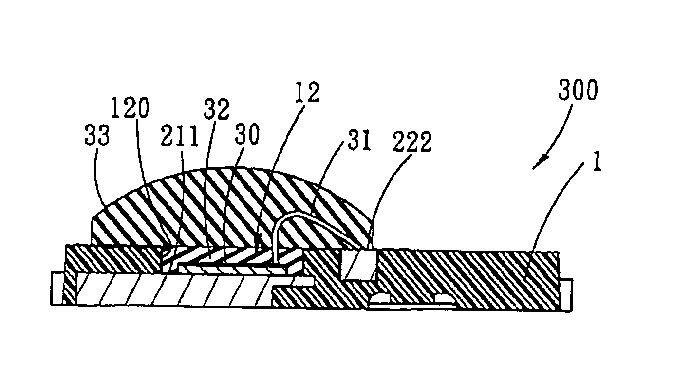
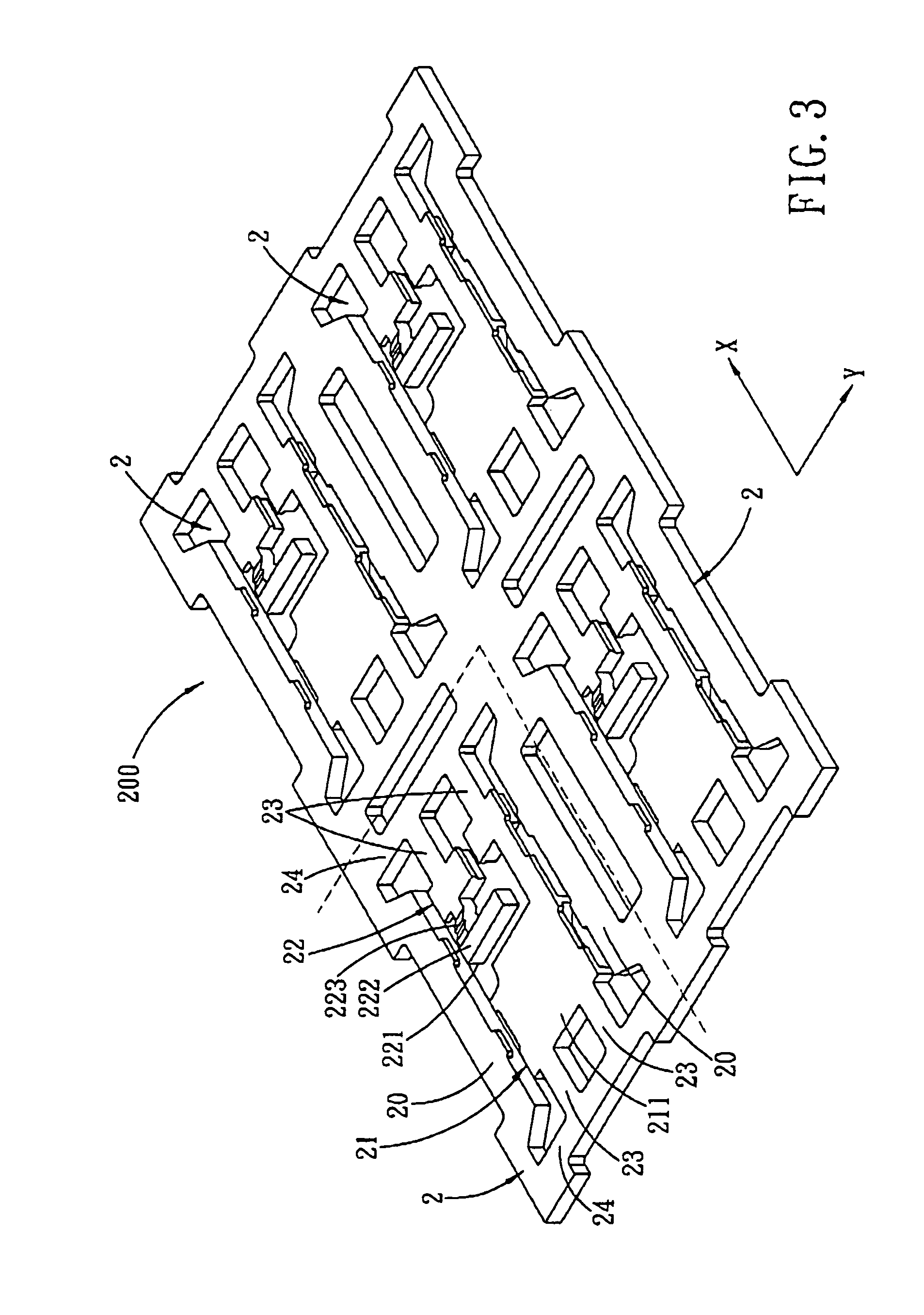
[0021]As shown in FIG. 3, a preferred embodiment of a lead frame assembly 200 according to the present invention comprises a plurality of lead frame units 2 connected to each other. Each of the lead frame units 2 includes a first lead frame portion 21, a second lead frame portion 22, a pair of first side strips 24, a pair of second side strips 20, and a plurality of connecting strips 23. The first side strips 24 of each of the lead frame units 2 are arranged in a first direction (X), and are aligned with and spaced apart from each other. The first side strips 24 of each of the lead frame units 2 extend along a second direction (Y) different from the first direction (X), and flank the first and second lead frame portions 21, 22 of a corresponding one of the lead frame units 2. The second side strips 20 of each of the lead frame units 2 are arranged in the second direction (Y), are aligned with and spaced apart from each other, and flank the first and second lead frame portions 21, 22...


PUM


Abstract

A package structure is adapted for mounting at least one light emitting diode (LED) die. The package structure includes an insulating housing having a top surface that is formed with a cavity, and a lead frame unit. The lead frame unit includes a first lead frame portion and a second lead frame portion. The first lead frame portion is covered by the insulating housing, and has a die-bonding area exposed within the cavity and adapted for mounting the LED die. The second lead frame portion is covered by the insulating housing, and has a conductive surface exposed outwardly of the top surface of the insulating housing and adapted for electrical connection with an end of a conductive wire.

Description

CROSS-REFERENCE TO RELATED APPLICATION[0001]This application claims priority of Chinese Patent Application No. 200910037562.2, filed on Feb. 26, 2009.BACKGROUND OF THE INVENTION[0002]1. Field of the Invention[0003]The invention relates to a lead frame assembly, more particularly to a lead frame assembly adapted for mounting light emitting diode (LED) dies, and a package structure having a lead frame unit of the lead frame assembly.[0004]2. Description of the Related Art[0005]Referring to FIG. 1, a conventional LED package structure 9 comprises a housing 92 formed with a cavity 921, and an LED die 91 mounted in the cavity 921. A conductive wire 93 has one end connected to the LED die 91, and the other end connected to a terminal 94 disposed in the cavity 921. The dimensions of the cavity 921 must be large enough to permit a wire binder (not shown) to be placed therein. However, such a large cavity 921 increases the thickness of the housing 92 and the size of the LED package structure...

Claims


Application Information

Patent Timeline
Patent Type & Authority Patents(United States)
IPC IPC(8): H01L31/0203H01L23/495
CPCH01L33/486H01L33/62H01L2224/49111H01L2924/01077H01L2924/15153H01L2924/1517H01L2224/48091H01L2924/00014H01L23/49541H01L24/48H01L24/49H01L24/97H01L2224/48227H01L2224/48247H01L2224/48472H01L2924/00H01L2924/12041H01L2224/73265H01L2224/8592H01L2224/45099H01L2224/45015H01L2924/207
Inventor LIN, CHEN-HSIU
Owner LITE ON TECH CORP
Features
  • R&D
  • Intellectual Property
  • Life Sciences
  • Materials
  • Tech Scout
  • Unparalleled Data Quality
  • Higher Quality Content
  • 60% Fewer Hallucinations
Learn More