Gate signal line drive circuit and display device

a technology of drive circuit and gate signal, which is applied in the direction of pulse technique, oscillation generator, reliability increasing modifications, etc., can solve the problem of unstable gate signal, and achieve the effect of suppressing the increase in circuit size and nois

Active Publication Date: 2013-06-04
JAPAN DISPLAY INC +1
View PDF9 Cites 6 Cited by
  • Summary
  • Abstract
  • Description
  • Claims
  • Application Information

AI Technical Summary

Problems solved by technology

When the shift register circuit that can perform bidirectional scanning has a plurality of basic circuits, which output predetermined gate signals, respectively, and controls the shift direction according to the phases of the clock signals, the following problem is caused when the basic circuits are reset by the gate signal of another basic circuit.
Further, when resetting is performed only by the two gate signals, the gate signals are not stable and cannot be maintained at a low voltage in the period of low voltage, which causes noises in the shift register circuit.

Method used


Image

  • Gate signal line drive circuit and display device
  • Gate signal line drive circuit and display device
  • Gate signal line drive circuit and display device

Examples


first embodiment

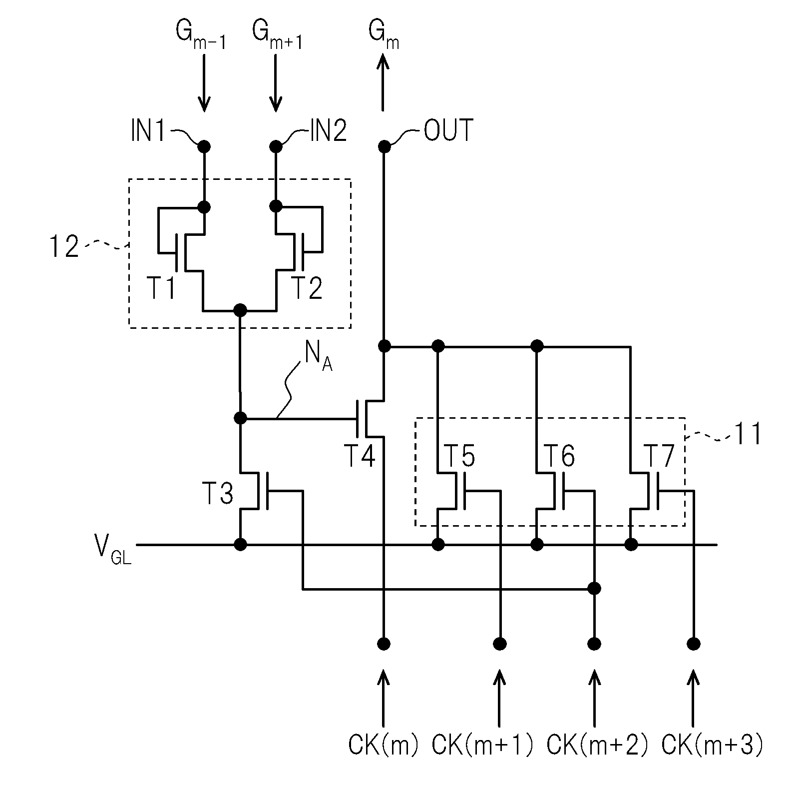
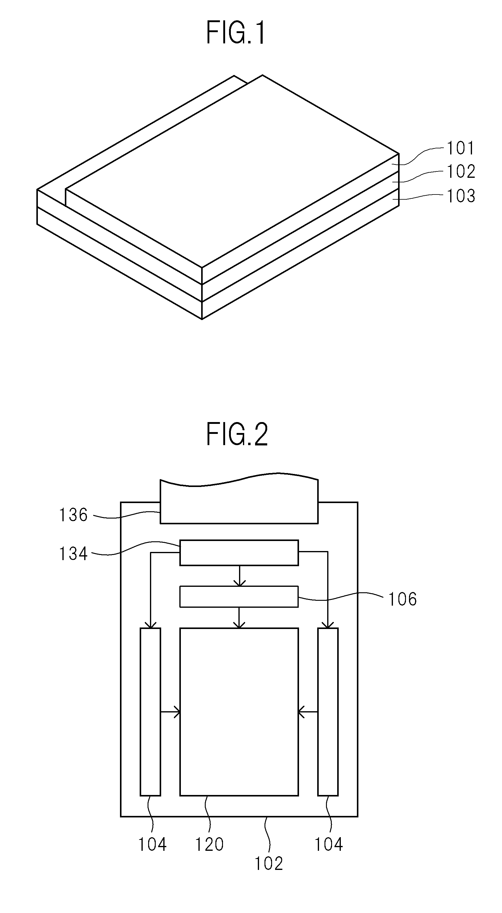
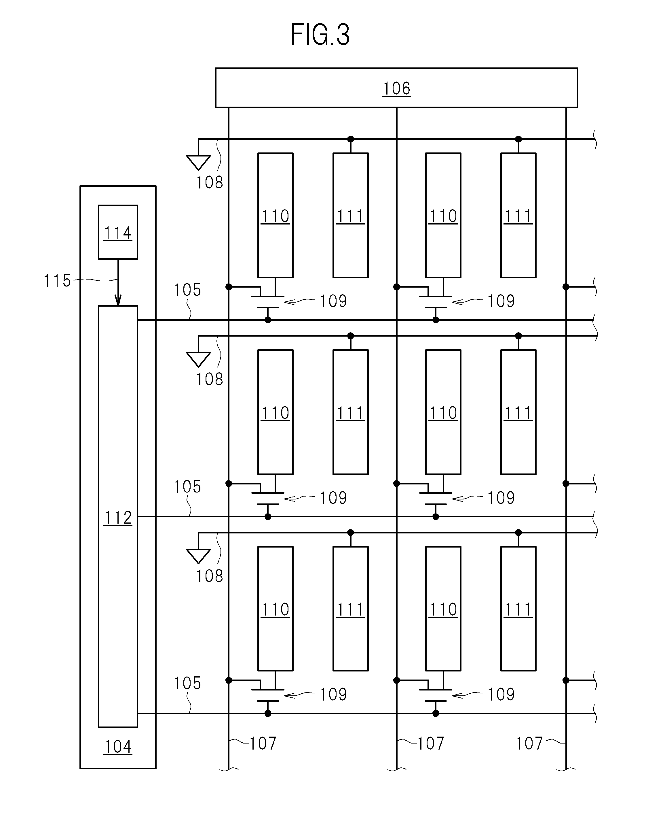
[0042]A display device according to a first embodiment of the present invention is, for example, an IPS (In-Plane Switching) liquid crystal display, and as shown in FIG. 1 which is a perspective view of the entire liquid crystal display, includes a TFT (Thin Film Transistor) substrate 102, a filter substrate 101 where a color filter is disposed, opposite to the TFT substrate 102, a liquid crystal material filled in the region between both of the substrates, and a backlight 103 disposed in contact with the opposite side to the filter substrate 101 of the TFT substrate 102. In this configuration, as described below, gate signal lines 105, video signal lines 107, pixel electrodes 110, common electrodes 111, and TFTs 109 are disposed on the TFT substrate 102 (see FIG. 3).

[0043]FIG. 2 is a block diagram showing the configuration of the liquid crystal display according to the embodiment. An FPC (Flexible Printed Circuit Board) 136 is connected to the TFT substrate 102 by press bonding and...

second embodiment

[0105]A display device according to a second embodiment of the present invention has the same configuration in detail as the display device according to the first embodiment. The main difference from the display device according to the first embodiment is the configuration of the basic circuit SR of the shift transistor 112.

[0106]FIG. 9 is a circuit diagram of the m-th basic circuit SR(m) of the shift register circuit 112 according to the embodiment. The main difference from the m-th basic circuit SR(m) according to the first embodiment, which is shown in FIG. 6, is that the configuration of the low-voltage applying switching circuit 11 is different and a second off-signal applying switching circuit (transistor T8) is further provided.

[0107]The low-voltage applying switching circuit 11 is three low-voltage applying switching elements (transistors T5, T7, and T10) which are connected in parallel with respect to the output terminal OUT. The m-th basic circuit SR(m) according to the fi...

third embodiment

[0119]A display device according to a third embodiment of the present invention has the same configuration in detail as the display device according to the second embodiment. The main difference from the display device according to the second embodiment is the configuration of the basic circuit SR of the shift transistor 112.

[0120]FIG. 11 is a block diagram of the shift register circuit 112 according to the embodiment. Similarly to FIG. 5, for brief description, when the shift register circuit 112 is composed of eight basic circuits SR arranged in a line is described.

[0121]The basic circuit SR is provided with four input terminals IN1, IN2, IN3, and IN4 and two output terminals OUT1 and OUT2. Similarly to the basic circuit SR shown in FIG. 5, the m-th basic circuit SR(m) outputs a gate signal Gm from the output terminal OUT1 and inputs a gate signal Gm−1 and a gate signal Gm+1 to the two input terminals IN1 and IN2, respectively. Further, according to the embodiment, the m-th basic ...


PUM


Abstract

Provided is a gate signal line driving circuit including: 2n clock signal lines where 2n-phase clock signals are input in the normal order of the sequence in normal-directional scanning and in the inverse order of the sequence in inverse-directional scanning, respectively; and a plurality of basic circuits, each being connected with the 2n clock signal lines and outputting a gate signal from an output terminal, in which each of the basic circuits includes a high-voltage applying switching circuit where one clock signal line is connected to an input side and applies a voltage applied to the clock signal line to the output terminal and an off-signal applying switching circuit that applies an off-voltage to a switch of the high-voltage applying switching circuit, and a clock signal line where a clock signal having an inverse phase is connected to a switch of the off-signal applying switching circuit.

Description

CROSS-REFERENCE TO RELATED APPLICATION[0001]The present application claims priority from Japanese application JP 2010-228672 filed on Oct. 8, 2010, the content of which is hereby incorporated by reference into this application.BACKGROUND OF THE INVENTION[0002]1. Field of the Invention[0003]The present invention relates to a gate signal line driving circuit and a display device using the gate signal line driving circuit. In particular, the present invention relates to a bidirectional driving that selects a normal sequence or an inverse sequence in response to an input clock signal and scans a gate signal line.[0004]2. Description of the Related Art[0005]In the related art, by enabling a gate signal driving circuit to scan a gate signal in any one of two directions, image display with a high degree of functionality, such as changing the direction of a displayed image, is made possible in a display device such as a liquid crystal display.[0006]A technology of driving a shift register c...

Claims


Application Information

Patent Timeline
Patent Type & Authority Patents(United States)
IPC IPC(8): H03B1/00H03K3/00
CPCG09G3/3677G09G3/00
Inventor SATO, HIDEOMAKI, MASAHIROABE
Owner JAPAN DISPLAY INC
Why Eureka
Try Eureka