

Solid-state imaging apparatus and driving method thereof
a solid-state imaging and driving method technology, applied in the field of solid-state imaging apparatus, can solve the problems of maintaining the withstand voltage of a mos transistor, dark current mixing into not giving satisfactory consideration to the amplitude of a pulse input to the gate electrode of the carrier accumulating portion,
- Summary
- Abstract
- Description
- Claims
- Application Information
AI Technical Summary
Problems solved by technology
Method used
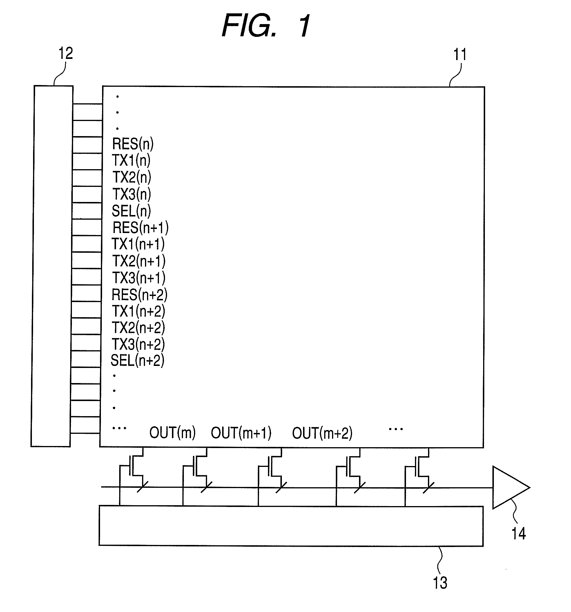
Image

Examples
first embodiment
(First Embodiment)
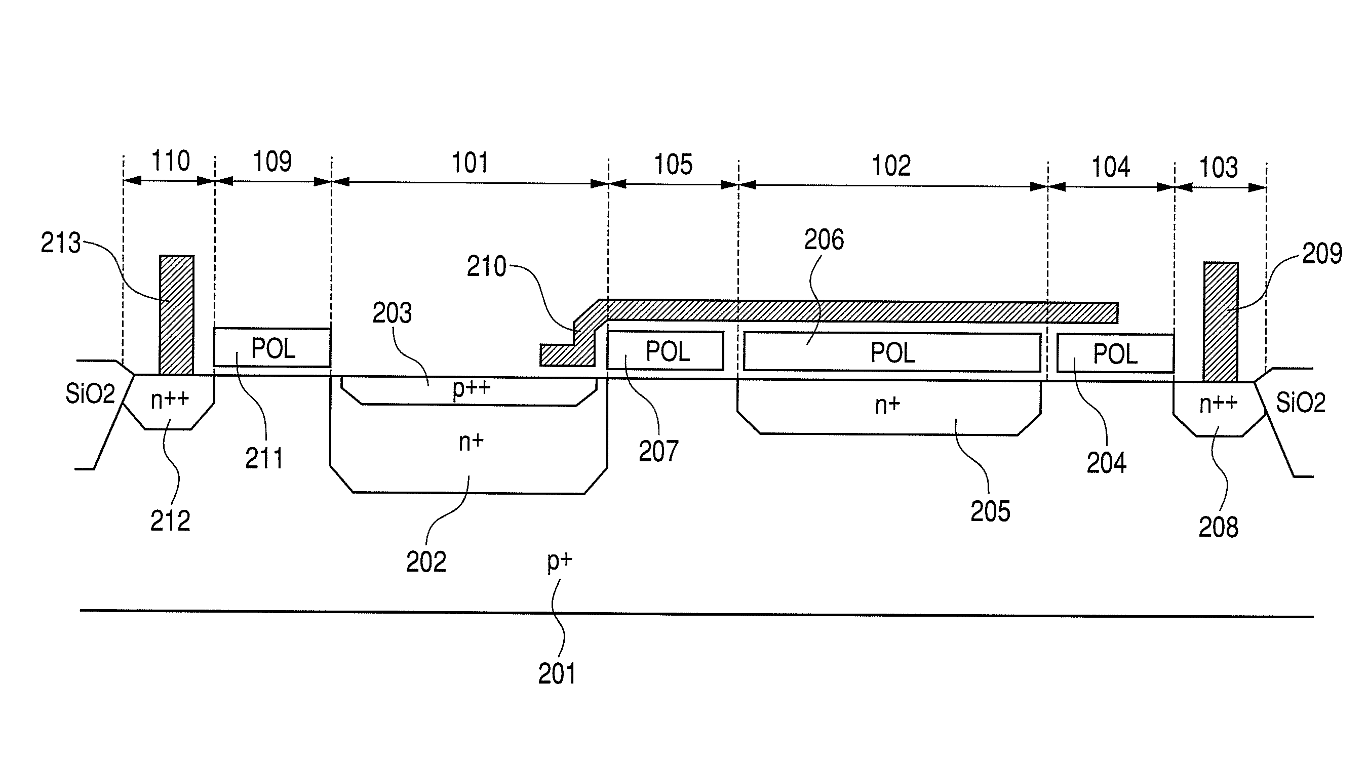
[0028]FIG. 3 is a plan view illustrating a solid-state imaging apparatus of the present embodiment. Although each region is illustrated as a rectangular shape for convenience of description, this does not mean that the structure of each region is rectangular. Rather, the figure shows that respective structures are at least arranged in these regions. The same applies to other embodiments.
[0029]For a photoelectric conversion portion 101, it is possible to use, for example, a photodiode. Incident light causes the generation of pairs of a signal carrier and a carrier opposite in polarity to the signal carrier.
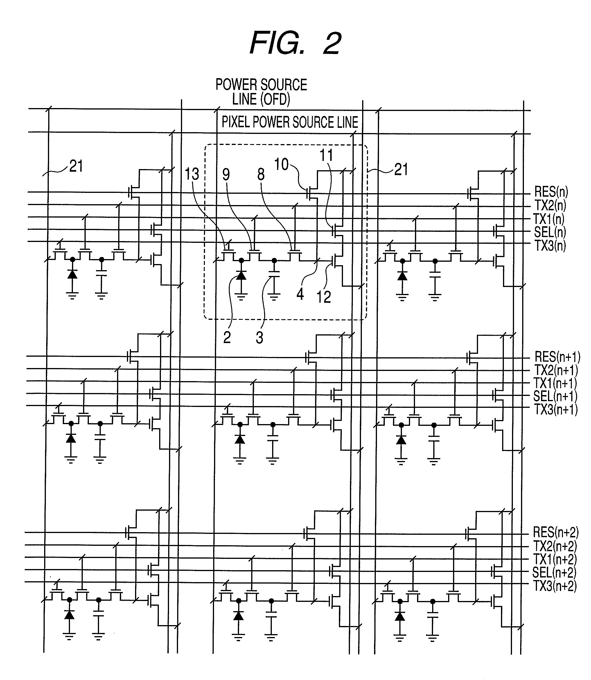
[0030]A carrier holding portion 102 is configured to be able to retain signal carriers generated in the photoelectric conversion portion. The carrier holding portion 102 includes a semiconductor region for accumulating signal carriers and a control electrode arranged over this semiconductor region through an insulating film.
[0031]A charge-to-voltage converting por...
second embodiment
(Second Embodiment)
[0077]FIG. 6 is a plan view of a solid-state imaging apparatus of the present embodiment, FIG. 7 is a cross-sectional view taken along the line 7-7 in FIG. 6, and FIG. 8 is a schematic view of driving pulses. Constituent elements having the same functions as those of the first embodiment are denoted by like reference numerals and will not be described in any more detail.
[0078]The present embodiment differs from the first embodiment in the structure of a path between the photoelectric conversion portion and the carrier holding portion. The path is structured so that carriers can be transferred from the photoelectric conversion portion to the carrier holding portion under the condition in which a voltage whereby the first transfer portion is placed in a non-conducting state is supplied. Specific examples of the structure include a buried channel structure provided underneath the second transfer electrode. In this structure, there exists a portion at a location deepe...
PUM
 Abstract
Description
Claims
Application Information