Solid state image pickup device and camera

a pickup device and solid-state image technology, applied in the direction of radio frequency controlled devices, television systems, instruments, etc., can solve the problems of accumulating carriers, noise easily generated, and being unable to read the signal of each pixel

Inactive Publication Date: 2008-01-22
CANON KK
View PDF47 Cites 156 Cited by
  • Summary
  • Abstract
  • Description
  • Claims
  • Application Information

AI Technical Summary

Problems solved by technology

Hence, it becomes impossible to read the signal of each pixel.
Moreover, because the carriers overflowed from the photodiode PD flow into the additional capacity CS through the floating diffusion FD, noises are easily generated due to the influence of the defects (damages) of the floating diffusion FD.
Consequently, in the floating diffusion FD, the accumulated carriers disappear owing to the defects, and great fixed pattern noises occur.

Method used


Image

  • Solid state image pickup device and camera
  • Solid state image pickup device and camera
  • Solid state image pickup device and camera

Examples


first embodiment

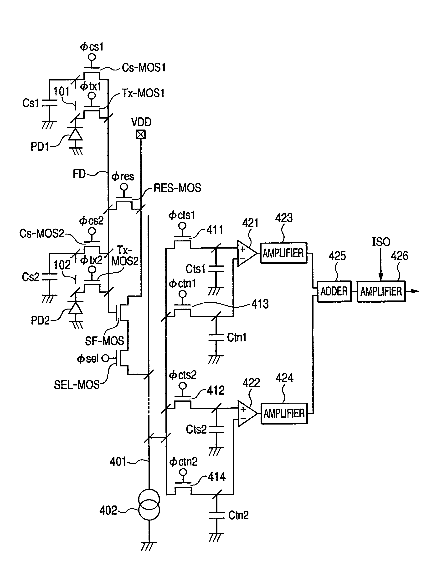
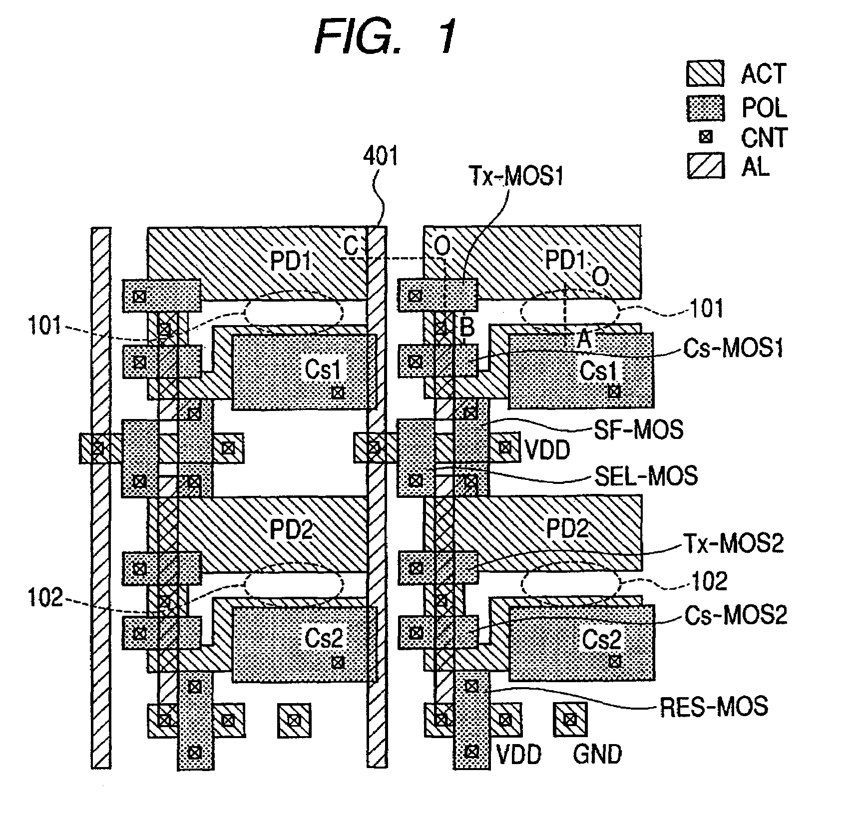
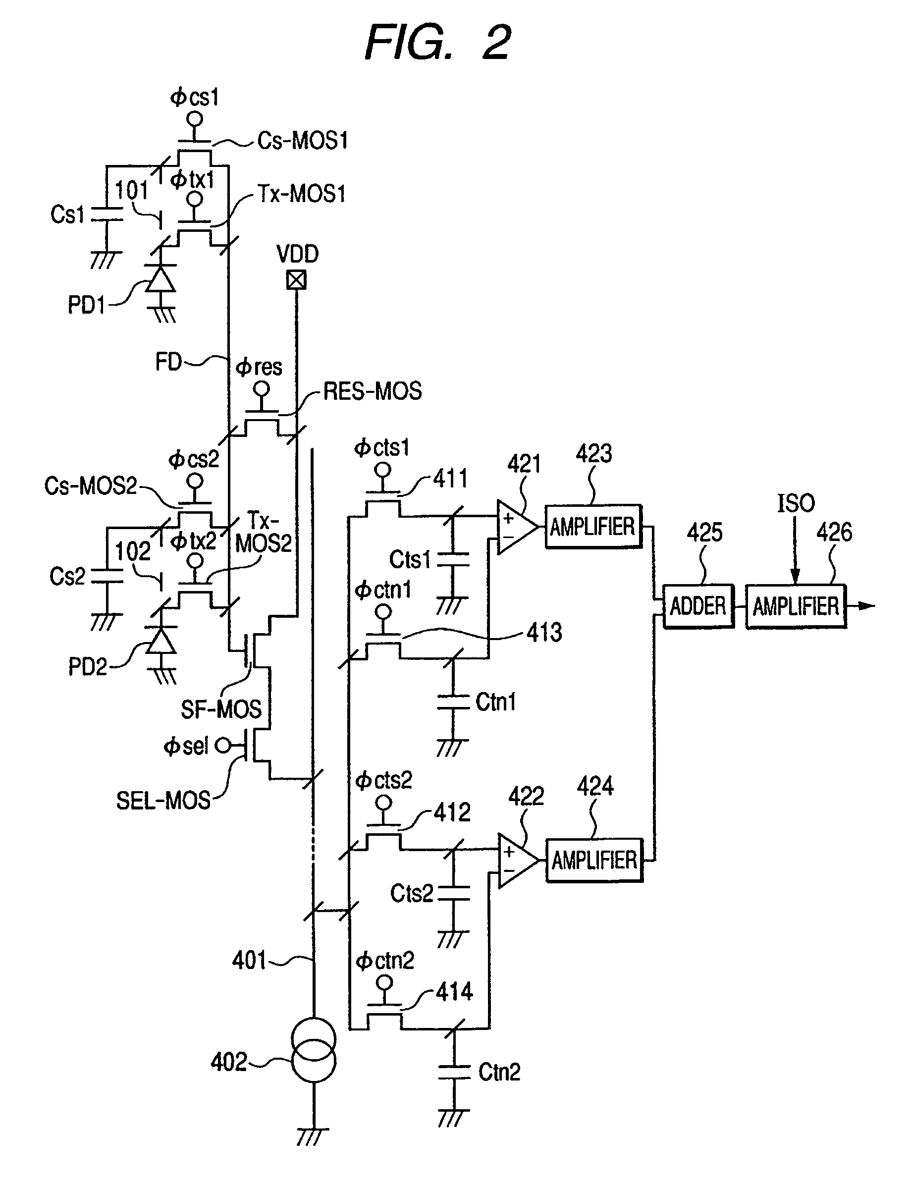
[0028]FIG. 1 is a layout chart showing an example of the whole configuration of a solid state image pickup device according to a first embodiment of the present invention, and FIG. 2 is an equivalent circuit diagram of the solid state image pickup device of FIG. 1.

[0029]In FIG. 1, the hatches drawn in the regions of photodiodes PD1 and PD2, and the like denote semiconductor regions (active regions) ACT. The hatches drawn in the regions of additional capacities Cs1 and Cs2, and the like denote polysilicon POL. The hatches drawn in the regions in wiring 401 and the like denote aluminum wiring AL. The hatches drawn in the regions in the portions connecting the wiring 401 with the semiconductor regions ACT and the like denote contact portions CNT.

[0030]The configuration of FIG. 2 is described. First, a first pixel structure is described. A photodiode (a first photoelectric conversion region) PD1 generates carriers by photoelectric conversions, and accumulates the generated carriers. A t...

second embodiment

[0074]FIG. 5 is a block diagram showing a configuration example of a still video camera according to a second embodiment of the present invention. Based on FIG. 5, an example of applying the solid state image pickup device of the first embodiment to a still video camera is described in detail. A solid state image pickup device 54 and an image signal processing circuit 55 correspond to the solid state image pickup device of the first embodiment.

[0075]A reference numeral 51 denotes a barrier to be commonly used as a protector of a lens and a main switch. A reference numeral 52 denotes a lens for forming an optical image of a subject on a solid state image pickup device 54. A reference numeral 53 denotes a diaphragm varying light quantity that has passed the lens 52 and a mechanical shutter. The reference numeral 54 denotes the solid state image pickup device for taking in the subject formed as an image by the lens 52 as an image signal. The reference numeral 55 denotes the image signa...

third embodiment

[0078]FIG. 6 is a block diagram showing a configuration example of a video camera according to a third embodiment of the present invention. Based on FIG. 6, an example of the case where the solid state image pickup device of the first embodiment is applied to the video camera is described in detail.

[0079]A reference numeral 1 denotes a taking lens equipped with a focus lens 1A for performing focusing, a zoom lens 1B for performing a zoom operation, and a lens 1C for forming an image. A reference numeral 2 denotes a diaphragm and mechanical shutter. A reference numeral 3 denotes a solid state image pickup device performing the photoelectric conversion of a subject image the image of which has been formed on an image pickup surface to convert the subject image into an electric image pickup signal. A reference numeral 4 denotes a sample hold circuit (S / H circuit) that performs the sample holding of the image pickup signal output from the solid state image pickup device 3 and further am...


PUM


Abstract

An solid state image pickup device including a plurality of photoelectric conversion regions (PD1, PD2) for generating carriers by photoelectric conversions to accumulate the generated carriers, an amplifying unit for amplifying the carriers, being commonly provided to at least two photoelectric conversion regions, a first and a second transfer units (Tx-MOS1, Tx-MOS2) for transferring the carriers accumulated in the first and the second photoelectric conversion regions, respectively, a first and a second carrier accumulating units (Cs1, Cs2) for accumulating the carriers flowing out from the first and the second photoelectric conversion regions through a first and a second fixed potential barriers, respectively, and a third and a fourth transfer units (Cs-MOS1, Cs-MOS2) for transferring the carriers accumulated in the first and the second carrier accumulating units to the amplifying unit, respectively.

Description

BACKGROUND OF THE INVENTION[0001]1. Field of the Invention[0002]The present invention generally relates to a solid state image pickup device and a camera, and more particularly to a solid state image pickup device the dynamic range of which is expanded.[0003]2. Description of Related Art[0004]FIG. 7 is a circuit diagram of a solid state image pickup device disclosed in Non-Patent Document 1 (Shigetoshi Sugawa et al. (five persons), “A 100 dB Dynamic Range CMOS Image Sensor Using a Lateral Overflow Integration Capacitor”, ISSCC 2005 / SESSION 19 / IMAGERS / 19.4, DIGEST OF TECHNICAL PAPERS, 2005 IEEE International Solid-State Circuit Conference, Feb. 8, 2005, pp. 352-353, 603.) FIG. 8 is a timing chart showing the operation of the solid state image pickup device. Hereinafter, an n-channel MOS field effect transistor is simply referred to as a transistor. FIGS. 9A, 9B, 9C, 9D, 9E and 9F are conceptual diagrams for illustrating the potential in a series of operations of the solid state image...

Claims


Application Information

Patent Timeline
Patent Type & Authority Patents(United States)
IPC IPC(8): H01L27/00H01L27/146H04N5/335H04N5/365H04N5/369H04N5/374H04N5/376
CPCH01L27/14603H01L27/14641H04N5/2173H04N5/37457H04N25/778H04N25/60
Inventor OKITA, AKIRAKOIZUMI, TORUOGURA, MASANORIKIKUCHI, SHINITANO, TETSUYA
Owner CANON KK
Why Eureka
Try Eureka