Quantum WELL MOS transistor and methods for making same

Inactive Publication Date: 2000-07-18
COMMISSARIAT A LENERGIE ATOMIQUE ET AUX ENERGIES ALTERNATIVES
View PDF7 Cites 156 Cited by
  • Summary
  • Abstract
  • Description
  • Claims
  • Application Information

AI Technical Summary

Problems solved by technology

This is a disadvantage when it is required to incre

Method used


Image

  • Quantum WELL MOS transistor and methods for making same
  • Quantum WELL MOS transistor and methods for making same
  • Quantum WELL MOS transistor and methods for making same

Examples


Embodiment Construction

The purpose of this invention is a quantum well MOS transistor and the processes for manufacturing this transistor which overcome the disadvantage mentioned above.

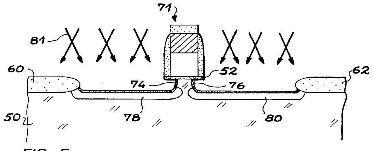
These processes are capable of aligning transistor source and drain areas on the grid of this transistor by selective etching.

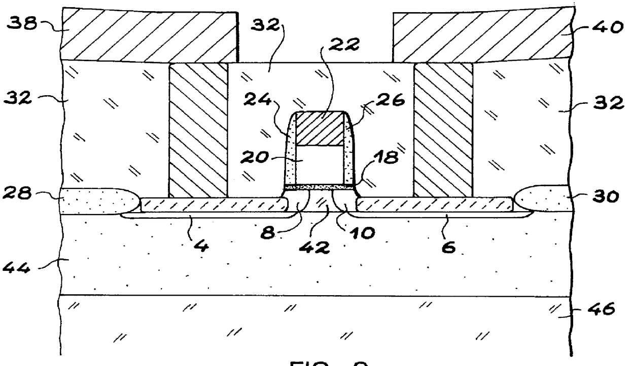
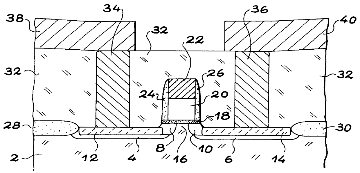
Specifically, the first purpose of this invention is a MOS type transistor comprising:

a semiconductor substrate,

a grid area,

a semiconductor channel located under the grid area and electrically insulated from it, and

a source area and a drain area that are located on each side of the grid area and the channel and which are electrically insulated from the substrate and the grid area,

this transistor being characterized in that the source and drain areas are separated from the channel by electrically insulating layers that are sufficiently thin to enable charge carriers to pass by means of the tunnel effect from the source area to the drain area through the channel, and in that each of the source and dra...


PUM


Abstract

PCT No. PCT/FR97/01075 Sec. 371 Date Feb. 12, 1998 Sec. 102(e) Date Feb. 12, 1998 PCT Filed Jun. 13, 1997 PCT Pub. No. WO97/48135 PCT Pub. Date Dec. 18, 1997A new quantum well MOS transistor is described along with a processes for manufacturing it. In this transistor, the source and drain areas are separated from the channel by sufficiently thin insulating layers to enable the passage of charge carriers by the tunnel effect. Each of the source and drain areas is separated from the substrate by an electrically insulating layer that is sufficiently thick to prevent charge carriers from passing through this insulating layer.

Description

This invention relates to a MOS (Metal-Oxide-Semiconductor) quantum well transistor and processes for manufacturing it.It has applications in microelectronics for manufacturing various devices, for example such as digital inverters that use MOS transistors complementary to each other.STATE OF PRIOR ARTFIG. 1 shows a schematic cross-sectional view of a conventional MOS transistor at the end of the integration process of forming this transistor.The transistor in FIG. 1 comprises a p type silicon substrate 2.Two areas 4 and 6 separated from each other are formed on this substrate 2.These areas 4 and 6 are n.sup.+ type diffused areas forming the transistor source and drain.As can be seen in FIG. 1, areas 4 and 6 are prolonged by areas 8 and 10 respectively, which are type n.sup.- diffused areas (less doped than areas 4 and 6).Areas 8 and 10 form extensions to the source and drain areas under the transistor grid that will be considered later.The transistor in FIG. 1 also comprises two ar...

Claims


Application Information

Patent Timeline
IPC IPC(8): H01L29/66H01L29/08H01L29/06H01L21/02H01L21/336H01L29/786H01L29/76H01L29/02H01L29/78
CPCB82Y10/00H01L29/0653H01L29/0847H01L29/0895H01L29/66636H01L29/66643H01L29/66772H01L29/7613H01L29/78618H01L29/78696H01L29/786
Inventor DELEONIBUS, SIMON
Owner COMMISSARIAT A LENERGIE ATOMIQUE ET AUX ENERGIES ALTERNATIVES
Why Eureka
Try Eureka