Decoration panel
a technology of decoration panel and light guide, which is applied in the direction of planar/plate-like light guide, lighting and heating apparatus, instruments, etc., can solve the problems of difficult to see painted colors and printed patterns, and unfavorable increase the thickness of the decoration panel, so as to reduce the volume of the decoration panel and achieve uniform illumination effect. , the effect of thinning the volum
- Summary
- Abstract
- Description
- Claims
- Application Information
AI Technical Summary
Benefits of technology
Problems solved by technology
Method used
Image
Examples
first embodiment
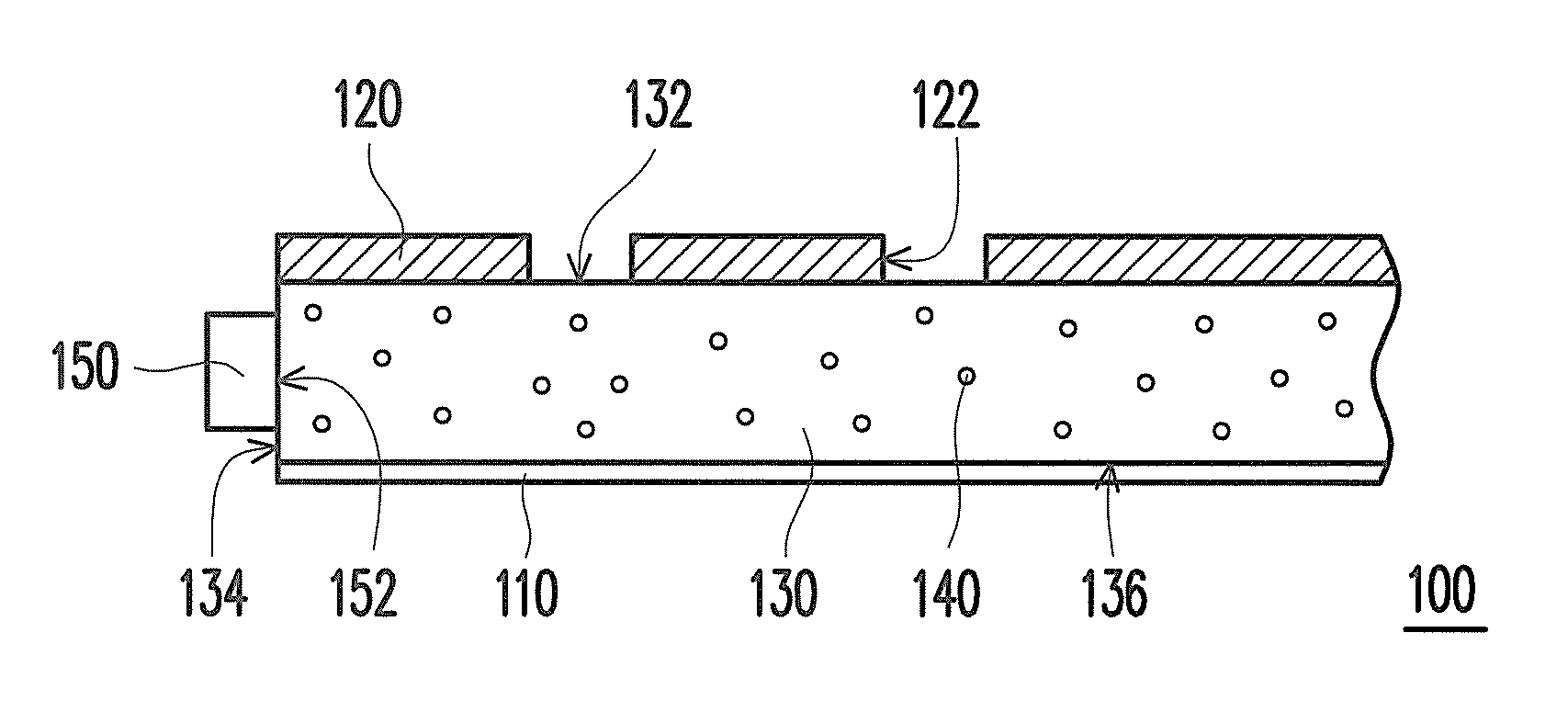
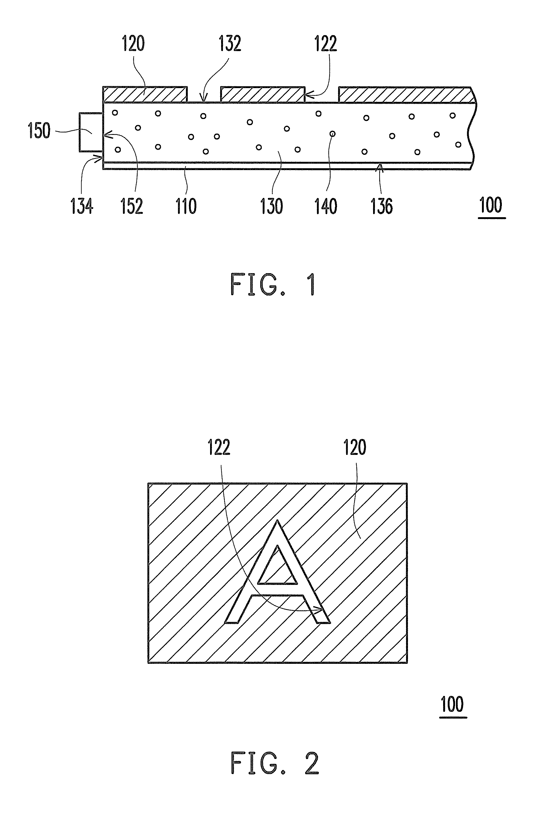
[0041]FIG. 1 schematically illustrates a cross-sectional view of a decoration panel according to the invention. Referring to FIG. 1, a decoration panel 100 includes a reflective layer 110, a light shielding pattern layer 120, a light guide 130, a plurality of diffusing particles 140, and a light emitting device 150. The light shielding pattern layer 120 is opposite to the reflective layer 110 and has a plurality of openings 122. The light guide 130 is disposed between the reflective layer 110 and the light shielding pattern layer 120. The plurality of diffusing particles 140 is distributed within the light guide 130. The light guide 130 has a light-exiting surface 132, a side surface 134, and a reflective surface 136. The light emitting device 150 is disposed beside the side surface 134 of the light guide 130 and the reflective layer 110 is disposed on the reflective surface 136 of the light guide 130 for reflecting the light to the light-exiting surface 132. In the present embodime...
third embodiment
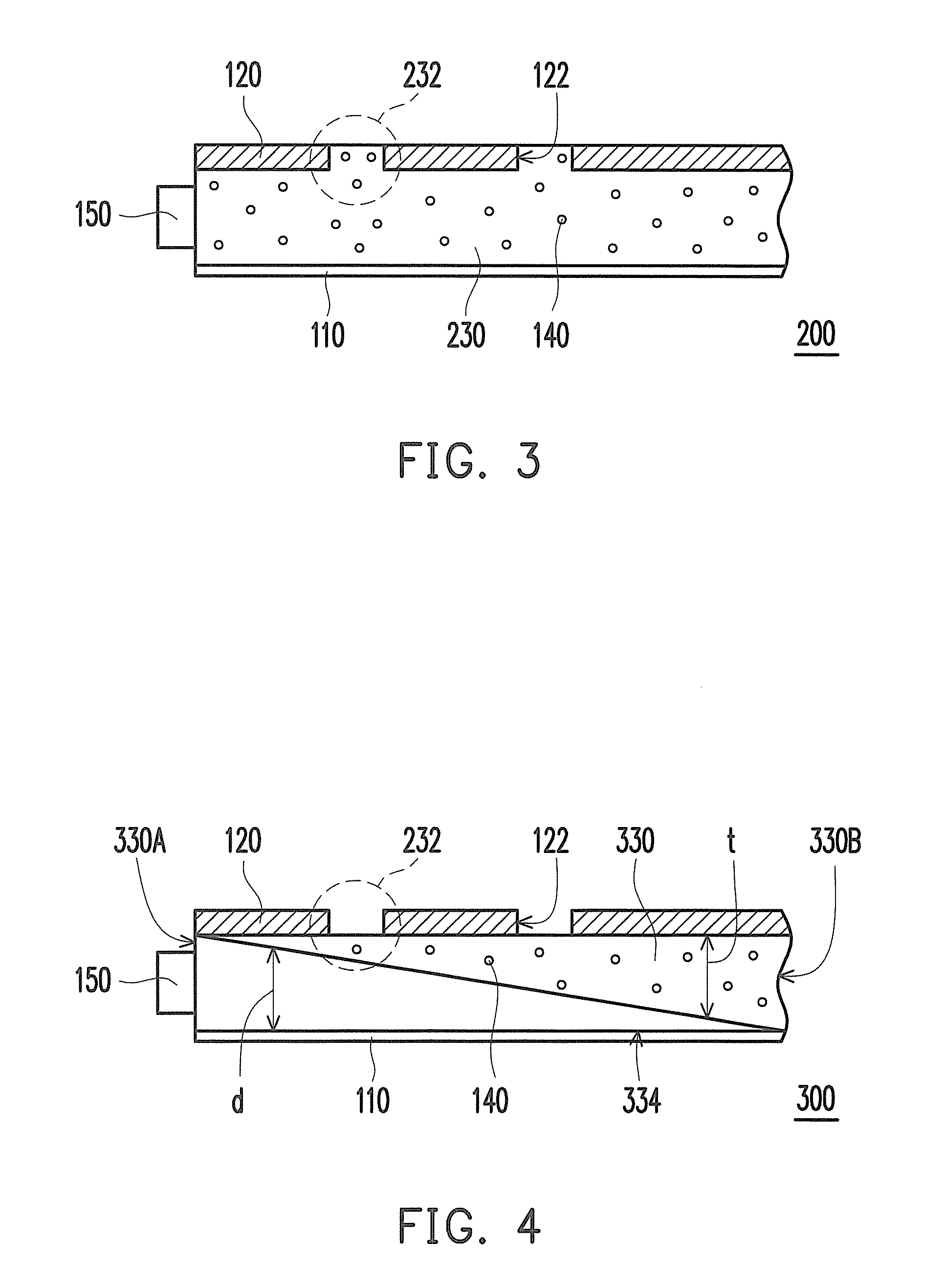
[0054]In addition, in the present embodiment, a thickness t of the light guide 430 is gradually decreased from a first side 430A of the light guide 430 adjacent to the light emitting device 150 toward a second side 430B opposite to the first side 430A. Furthermore, a distance d from the reflective layer 110 to the light guide 430 is, on the contrary, gradually increased with the decrease of the thickness t of the light guide 430. Similar to the third embodiment, the wedge-shaped light guide 430 conduces to change the transmission direction of the light beam emitted from the light emitting device 150. Therefore, the decoration panel 400 can have even brightness represented in different openings 122 without disposing any additional diffusing element therein. In specific, the wedge-shaped light guide 430 can have a substantially flat reflective surface (not marked) facing to the reflective layer 110 and no diffusing structure or diffusing pattern is required to be disposed on the subst...
seventh embodiment
[0062]FIG. 8 schematically illustrates a cross-sectional view of a decoration panel according to the invention. Referring to FIG. 8, the decoration panel 700 includes a light guide 710, a plurality of diffusing particles 720, a reflective layer 730, and a light emitting device 740. The light guide 710 includes a first portion 712 and a second portion 714 connected to the first portion 712. The diffusing particles 720 are distributed within the second portion 714 of the light guide 710. The reflective layer 730 is disposed at a side of the first portion 712 away from the second portion 714. The light emitting device 740 is disposed beside the first portion 712 of the light guiding plate 710 and the light emitting device 740 can be a light bar, a lamp, or a cold cathode lamp.
[0063]In the present embodiment, the light emitting device 740 is used for providing light to achieve the illumination of the decoration panel 700. Therefore, the light beam emitted from the light emitting device ...
PUM
 Abstract
Description
Claims
Application Information


