

Arylsulfonic acid compound and use thereof as electron-acceptor material
a technology of arylsulfonic acid and electron acceptor, which is applied in the direction of non-metal conductors, conductors, organic chemistry, etc., can solve the problems of reducing the character of the compound, limiting the choice of solvent, and limiting the coating method to ensure uniform film formation, so as to achieve uniform emission face, improve emission current efficiency, and high solubility
- Summary
- Abstract
- Description
- Claims
- Application Information
AI Technical Summary
Benefits of technology
Problems solved by technology
Method used
Image

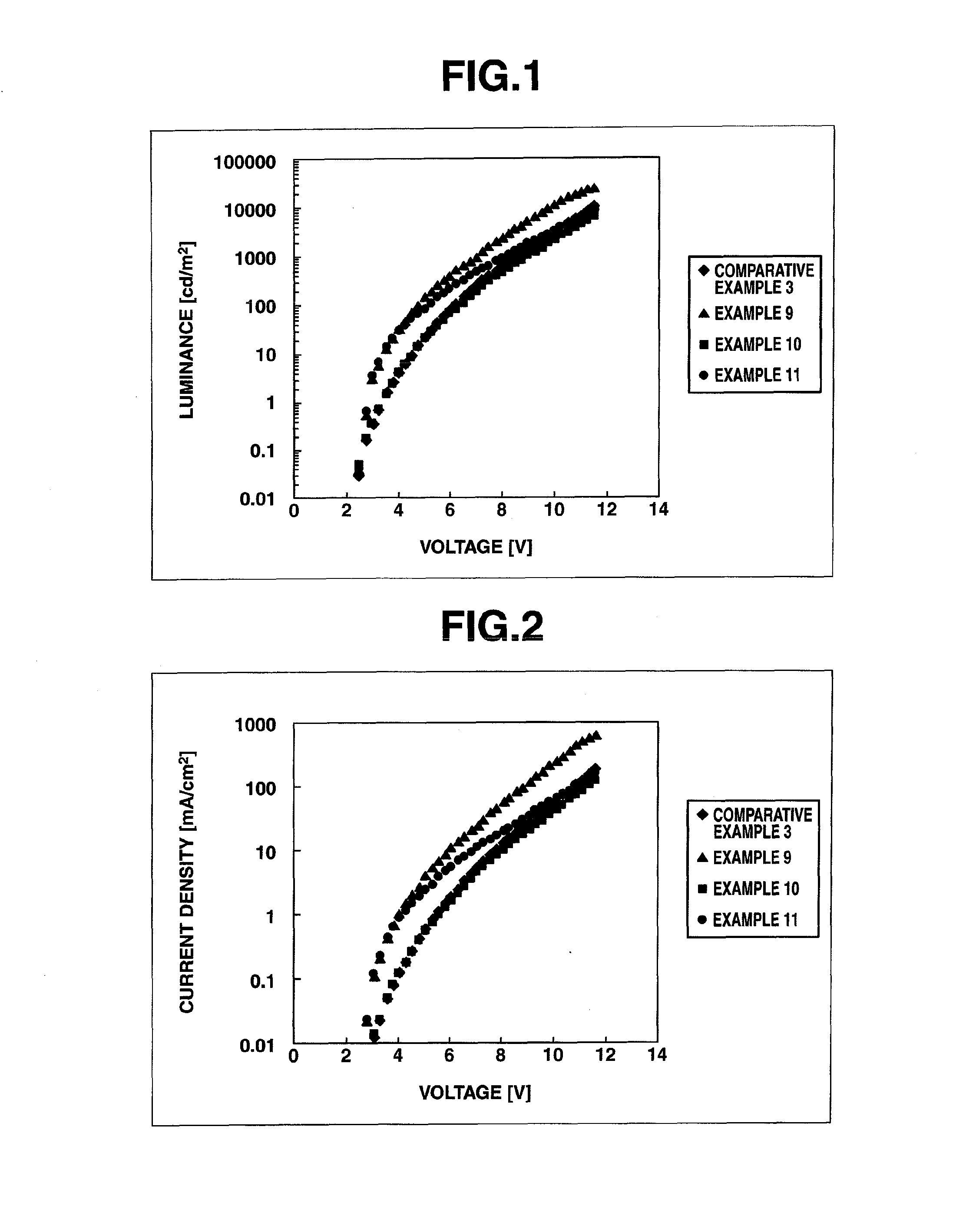
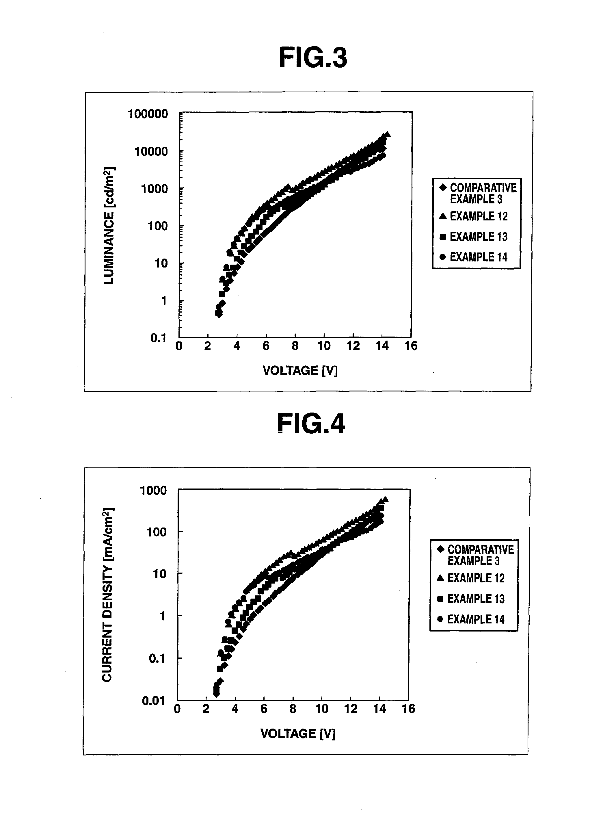
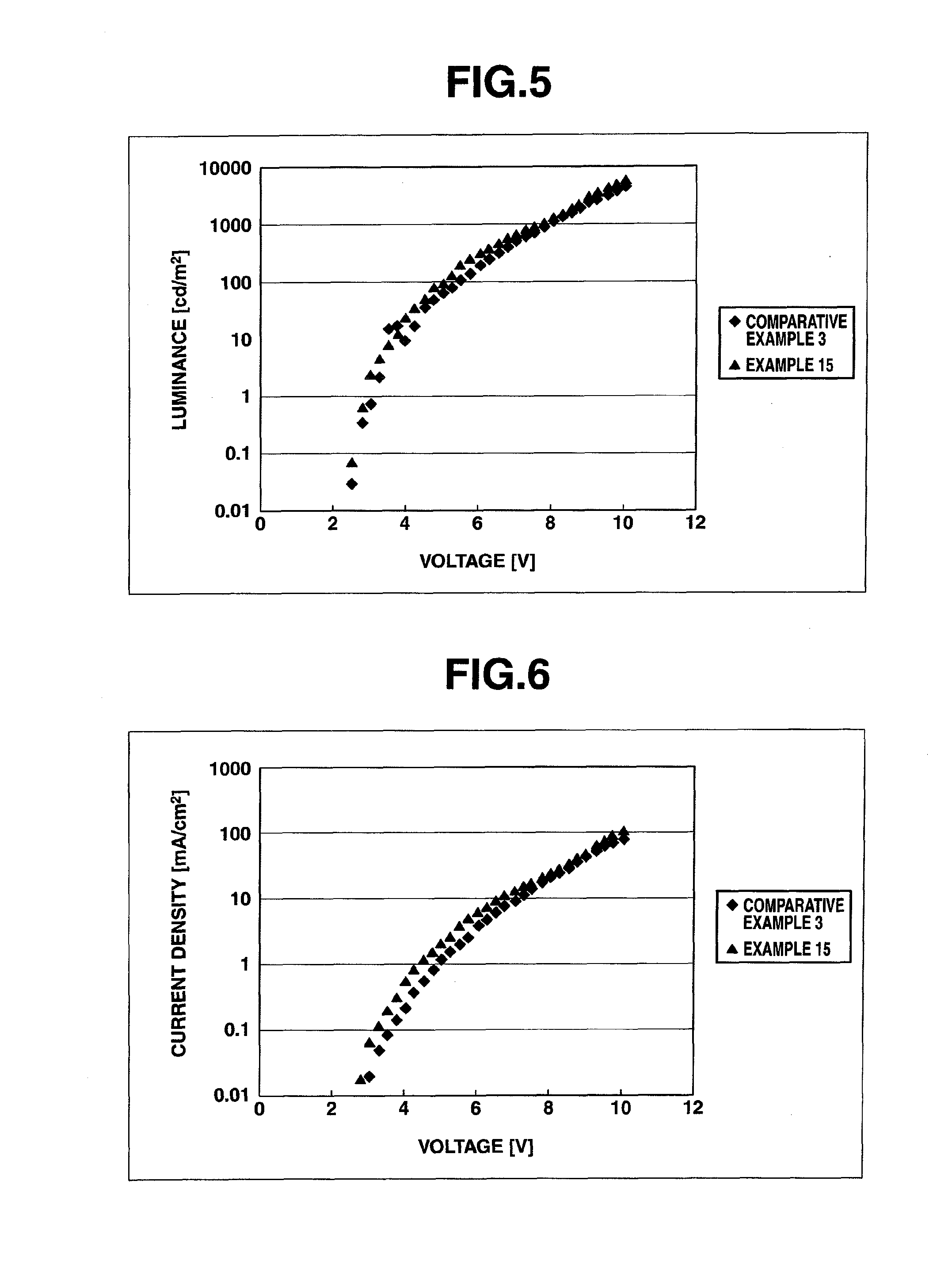
Examples
synthetic example 1
Synthesis of Phenyltetraaniline
[0139]
[0140]Phenyltetraaniline (PTA) was obtained according to the following procedure based on the method set forth in Bulletin of Chemical Society of Japan, 1994, Vol. 67, pp. 1749-1752.
[0141]In 2 liters of toluene, 12.977 g of p-phenylenediamine was dissolved, to which 245.05 g of tetra-n-butoxy titanium serving as a dehydration condensing agent was added, followed by dissolution at 70° C. for 30 minutes. Thereafter, 53.346 g of p-hydroxydiphenylamine was added, followed by reaction at a reaction temperature of 100° C. for 24 hours. After completion of the reaction, the reaction solution was filtered and the resulting filtrate was washed successively with toluene and ether and dried to obtain silver crystals. Then, 25 parts by weight of dioxane and 0.2 equivalents of hydrazine monohydrate, relative to the resulting crystals, were added and the reaction system was purged with nitrogen, followed by heating under reflux to dissolve the crystals. To the...
example 1
[0143]Perfluorotoluene naphthalenesulfonic acid compound (hereinafter abbreviated as 7FNS-1) was synthesized according to the following reaction formula.
[0144]
[0145]Under nitrogen atmosphere, 6.78 g of perfluorotoluene, 4.37 g of potassium carbonate and 500 ml of N,N-dimethylformamide were successively added to 10 g of sodium 1-naphthol-3,6-disulfonate (made by Tokyo Chemical Industry Co., Ltd.) and the reaction system was purged with nitrogen, followed by agitation at 100° C. for 5 hours.
[0146]After 5 hours, filtration was carried out so as to remove the potassium carbonate. The resultant residue was added with 50 ml of methanol and washed for 30 minutes, followed by filtration of the suspension. The resulting filtrate was concentrated to dryness under reduced pressure, to which 500 ml of pure water was added for dissolution, followed by purification through column chromatography using cationic exchange resin Dowex 650C (about 200 ml of H type, distillate solvent: water).
[0147]The ...
example 2
[0150]Perfluoroallylbenzene naphthalenesulfonic acid compound (hereinafter abbreviated as 9FNS-1) was synthesized according to the following reaction formula.
[0151]
[0152]In the same manner as in Example 1 except that 3.08 g of 3-(pentafluorophenyl)pentafluoro-1-propene, 1.31 g of potassium carbonate and 150 ml of N,N-dimethylformamide were successively added to 3 g of sodium 1-naphthol-3,6-disulfonate (made by Tokyo Chemical Industry Co., Ltd.) and the reaction system was purged with nitrogen, followed by agitation at 100° C. for 5 hours, 3.1 g of a white powder (yield: 62%) was obtained.
[0153]Molecular weight: 582.37
[0154]MALDI-TOF; 581.0 [M-H]−
PUM
| Property | Measurement | Unit |
|---|---|---|
| boiling point | aaaaa | aaaaa |
| boiling point | aaaaa | aaaaa |
| boiling point | aaaaa | aaaaa |
Abstract
Description
Claims
Application Information