Ceramic capacitor and method of manufacturing same
a ceramic capacitor and capacitor technology, applied in the field of ceramic capacitors, can solve the problems of large changes in the thickness dimension of ceramic dielectric layers, difficult to precisely control this thickness dimension, and suffers in the conventional ceramic capacitor described above, so as to enhance the orientation stability of the internal electrode and increase the capacitance
- Summary
- Abstract
- Description
- Claims
- Application Information
AI Technical Summary
Benefits of technology
Problems solved by technology
Method used
Image
Examples
first embodiment
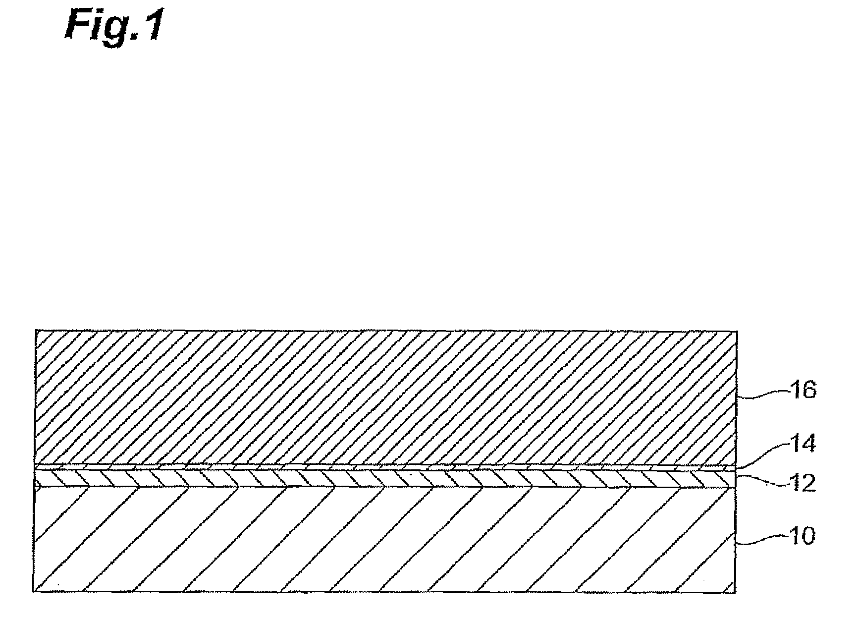
[0048]When manufacturing a ceramic capacitor related to the first embodiment of the present invention, first, as shown in FIG. 1, an Al2O3 insulation layer 12, Ni seed layer (first seed layer) 14, and thick-film photoresist masking layer 16 are sequentially stacked on top of a substrate 10 (for example, a silicon substrate). The seed layer 14 is 1000Å thick, and the masking layer 16 is 6 μm thick.
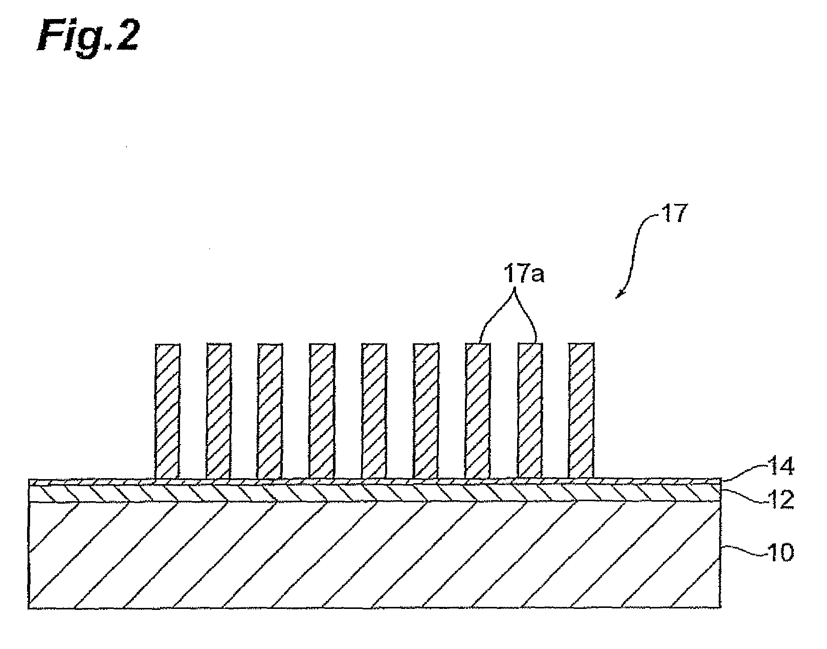
[0049]Next, as shown in FIG. 2, patterning of the masking layer 16 is carried out using a known photoresist technique to form a thick-film mask (first thick-film mask) 17. The thick-film mask 17 comprises a plurality of mask strips 17a between 0.4 and 0.6 μm wide extending perpendicularly relative to the surface of the substrate 10, and, for example, this plurality of mask strips 17a is arranged regularly at clearances of between 0.6 and 0.8 μm.
[0050]Then, as shown in FIG. 3, Ni plating of the seed layer 14 is carried out to form a plated layer 18A. This plated layer 18A is formed 5.5 μm th...
second embodiment
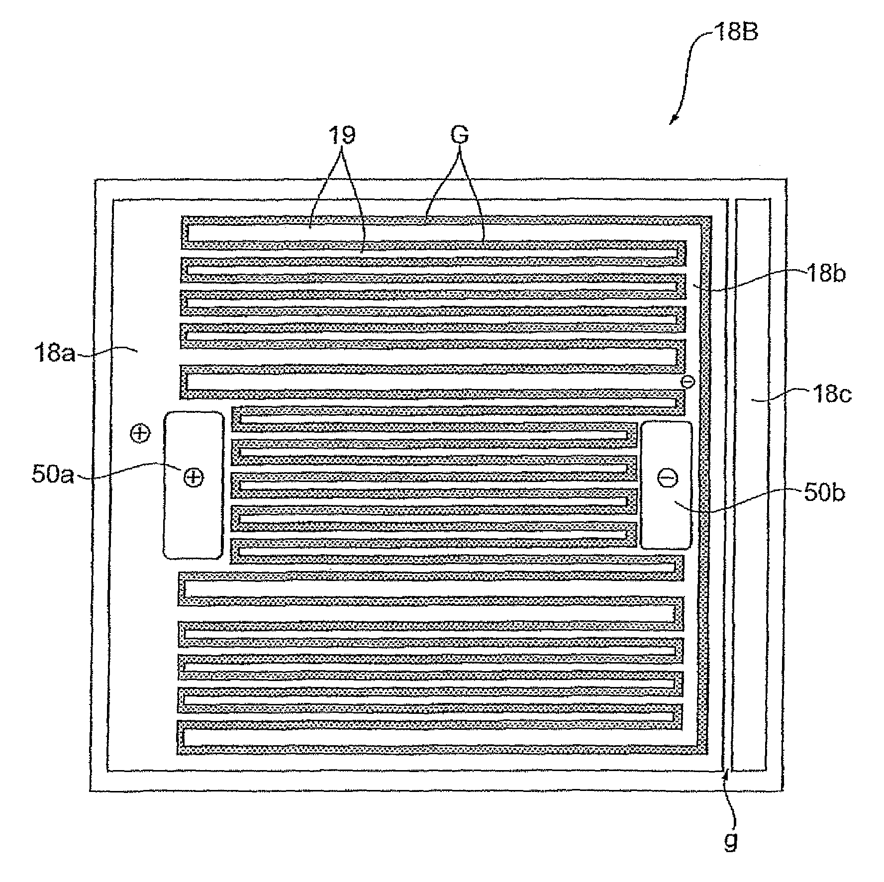
[0075]Next, a ceramic capacitor 1B related to a second embodiment of the present invention will be explained. This ceramic capacitor 1B, as shown in FIG. 13, constitutes a two-tiered ceramic capacitor comprising internal electrodes 18a, 18b, 18c in the first tier, and internal electrodes 38a, 38b, 38c in the second tier.
[0076]The steps for manufacturing the ceramic capacitor 1B will be explained below.
[0077]When manufacturing ceramic capacitor 1B, first, patterned internal electrodes 18a, 18b, 18c are formed on top of a substrate 10 in accordance with the same steps as those in the first embodiment. That is, subsequent to sequentially layering a Al2O3 insulation layer 12, a Ni seed layer (first seed layer) 14, and a thick-film photoresist masking layer 16 on top of the substrate 10, masking layer 16 patterning is carried out using a known photoresist technique to form a thick-film mask 17. Then, subsequent to carrying out the Ni plating of the seed layer 14 to form a plated layer 18...
PUM
| Property | Measurement | Unit |
|---|---|---|
| thick | aaaaa | aaaaa |
| thick | aaaaa | aaaaa |
| width | aaaaa | aaaaa |
Abstract
Description
Claims
Application Information


