Method and device for marking a surface using controlled periodic nanostructures

Active Publication Date: 2013-06-25
ADVANCED TRACK TRACE
View PDF8 Cites 3 Cited by
  • Summary
  • Abstract
  • Description
  • Claims
  • Application Information

AI Technical Summary

Benefits of technology

[0032]According to particular features, during the electronic image capture step, a light source is oriented to illuminate the marked image with a pre-defined orientation. Thanks to these provisions, the reading of the code is improved.
[0033]According to particular features, the reading method that is the subject of this invention, as described in brief abo

Problems solved by technology

These marking means are very suitable for serial markings but offer low security with respect to identifying or authenticating the object or document marked.
As a result of these two characteristics, t

Method used


Image

  • Method and device for marking a surface using controlled periodic nanostructures
  • Method and device for marking a surface using controlled periodic nanostructures
  • Method and device for marking a surface using controlled periodic nanostructures

Examples


first embodiment

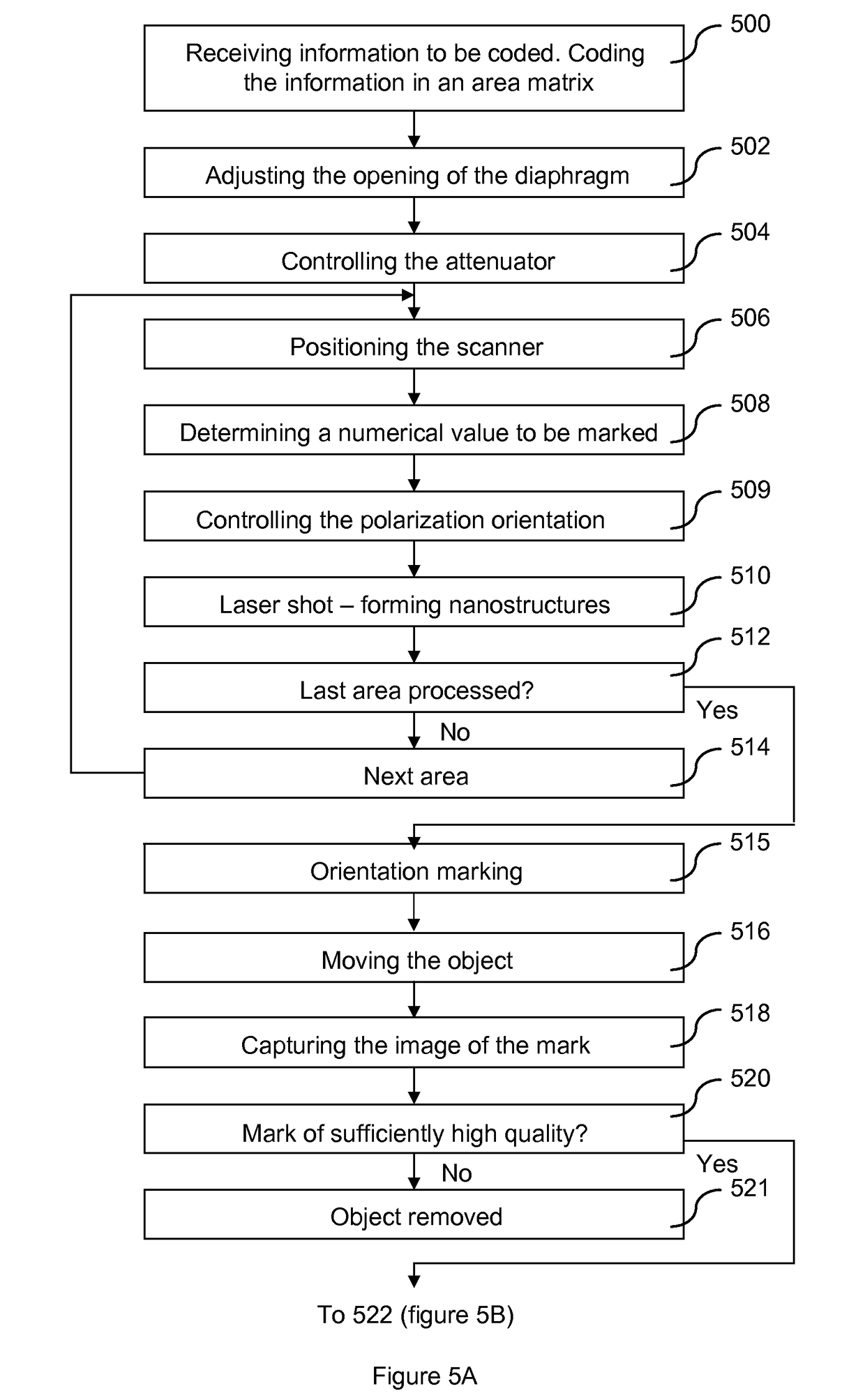
[0073]In this invention, the device for marking a mold is utilized, all the items molded with this mold reproducing the nanostructure realized with the device on the mold. It is noted that this serial manufacturing nevertheless allows the molded items to be individually identified. For this purpose, an image of the nanostructure is captured and the position of random molding errors is determined and then the distribution of these random errors. This distribution is then stored, for example in a database that can be accessed remotely, for example via the Internet network, in association with an identifier of the item (for example, a date of manufacture, batch or individual serial number). During the subsequent recognition of the item to identify, an image of the nanostructure is again captured, the position and distribution of the molding errors are determined and this distribution is compared with those stored in memory to identify the item by the other data stored with regard to th...

second embodiment

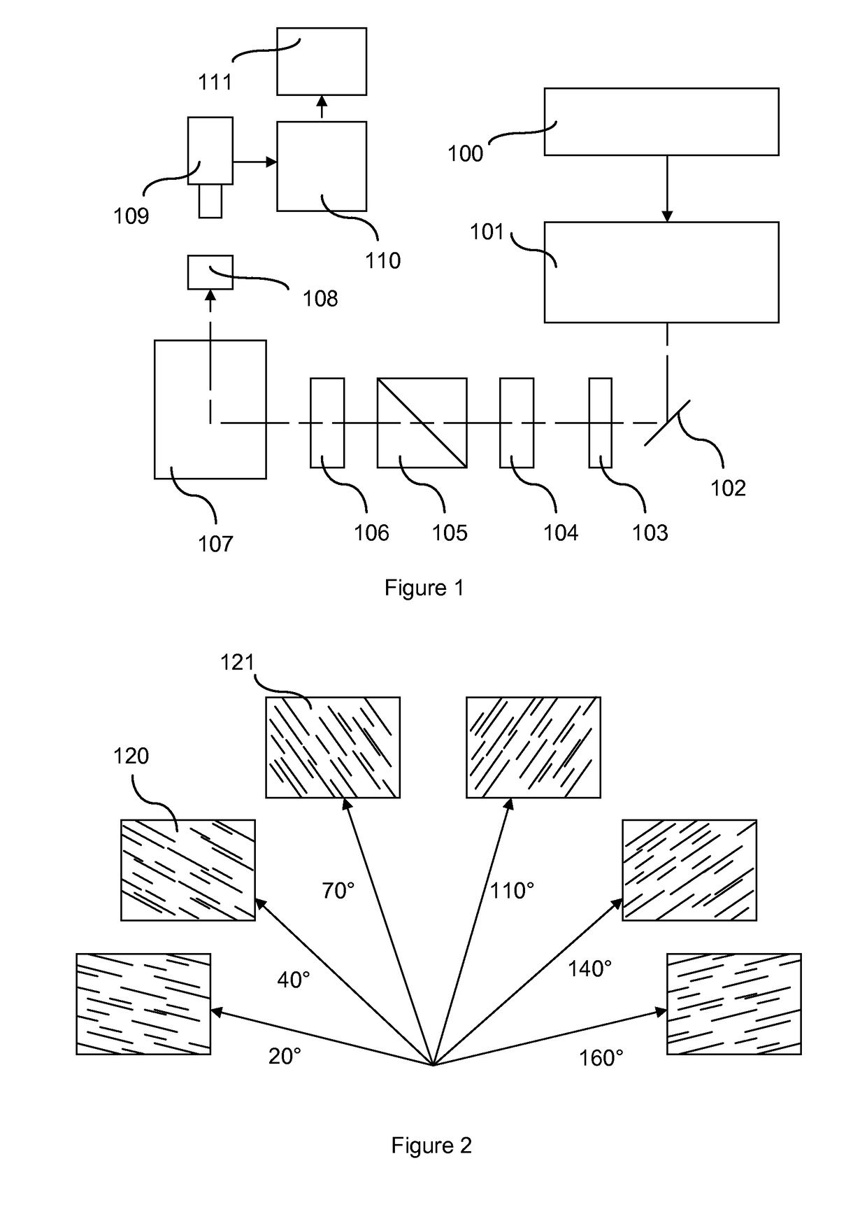
[0074]In the device that is the subject of this invention, each object, or document, is individually the object of a marking by the device, the image and the mark thus formed varying, independent of the marking errors, from one object to the next or one batch to the next.

[0075]FIG. 2 shows that, according to the polarization angle of the laser beam, represented on arrows leading to images of nanostructures, the orientation of the nanostructures varies. For example, the longest lines of nanostructure 120, realized with a polarization angle of 40° with respect to the horizontal, are oriented at approximately 40° and the longest lines of nanostructure 121, realized with a polarization angle of 70° with respect to the horizontal, are oriented at approximately 70°. However these angles are measured from two perpendicular straight lines. In effect, the lines of nanostructure 121 are noticeably perpendicular to the polarization plane of the light from the laser.

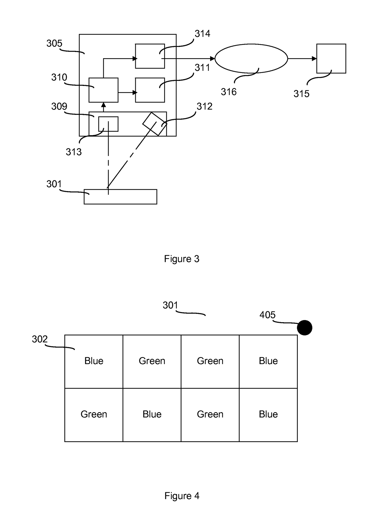
[0076]FIG. 3 shows an inform...


PUM


Abstract

A method for marking a surface by controlled periodic nanostructures includes:
    • a step (500) of coding an item of information in the form of an image including values representative of the coded information and
    • a step (506 to 514) of marking, dot by dot, an area of the surface with a polarized laser beam to form oriented nanostructures on or in the surface, by modulating the laser beam's polarization for each marking dot according to the value of a dot of the image. In embodiments, during the marking step, a pulsed laser is utilized with a duration of less than 10×10−12 seconds and an element of polarizing the light coming from the laser source and reaching the surface, designed to polarize the light according to a polarization axis that can vary according to a signal received by the polarization element, is utilized.

Description

[0001]The present invention concerns a method and a device for marking a surface by controlled periodic nanostructures and a method and a device for reading information on such a surface. It applies, in particular, to marking an object or a document with a view to its identification, traceability and authentication.[0002]A large number of marking means are known, for example by printing or by modifying a surface state. These marking means are very suitable for serial markings but offer low security with respect to identifying or authenticating the object or document marked. In particular, it is generally easy for a counterfeiter to reproduce them.[0003]In addition, markings of the prior state of the art are generally visible, which facilitates their detection, analysis or destruction by a counterfeiter.[0004]The existence of periodic structures, having a period of several hundred nanometers, has been highlighted scientifically (see, for example, the document by Messrs. GUILLERMIN, F...

Claims


Application Information

Patent Timeline
IPC IPC(8): B41J2/47
CPCG06K5/02G06K1/12
Inventor AUDOUARD, ERICFOUCOU, ALAINMASSICOT, JEAN-PIERRESAGAN, ZBIGNIEWDUSSER, BENJAMINJOURLIN, MICHELSODER, HERVE
Owner ADVANCED TRACK TRACE
Why Eureka
Try Eureka