Buffer operational amplifier with self-offset compensator and embedded segmented DAC for improved linearity LCD driver

a buffer operational amplifier and self-offset compensation technology, applied in pulse generators, instruments, pulse techniques, etc., can solve the problems of parasitic capacitance at the input terminal of the op-amp that has an undesirable effect on the output of the dac, and the linearity of the dac is worsening with increasing resolution, so as to reduce the offset of the operational amplifier

Active Publication Date: 2013-07-02
TAIWAN SEMICON MFG CO LTD
View PDF21 Cites 25 Cited by
  • Summary
  • Abstract
  • Description
  • Claims
  • Application Information

AI Technical Summary

Benefits of technology

[0009]A driver includes a digital-to-analog converter (DAC) having a digital input representing an input voltage between first and second analog voltage levels and an analog output. An operational amplifier has an output and first and second inputs. The first input has a first differential input pair of transistors including a first NMOS transistor and a first PMOS transistor. The second input has a second differential input pair of transistors including a second NMOS transistor and a second PMOS transistor. Switching logic is used to reduce offset in the operational amplifier. The switching logic is operable to selectively couple: the first NMOS and PMOS transistors to the analog output of the DAC and the second NMOS and PMOS transistors to the operational amplifier output when the input voltage is between a low reference voltage and a high reference voltage; the first and second NMOS transistors to an intermediate voltage between the low and high reference voltages, the first PMOS transistor to the analog output of the DAC and the second PMOS transistor to the operational amplifier output when the input voltage is below the low reference voltage; and the first and second PMOS transistors to the intermediate voltage, the first NMOS transistor to the analog output of the DAC and the second NMOS transistor to the operational amplifier output when the input voltage is above the high reference voltage.

Problems solved by technology

Other problems also exist with conventional DACs.
Unfortunately, parasitic capacitance at an input terminal of the OP-AMP has an undesirable effect on an output of the DAC, namely off-set, when modulating a voltage level of a non-inverting input terminal of the OP-AMP.
However, with this architecture the DAC linearity worsens with increases in resolution.

Method used


Image

  • Buffer operational amplifier with self-offset compensator and embedded segmented DAC for improved linearity LCD driver
  • Buffer operational amplifier with self-offset compensator and embedded segmented DAC for improved linearity LCD driver
  • Buffer operational amplifier with self-offset compensator and embedded segmented DAC for improved linearity LCD driver

Examples


Embodiment Construction

[0023]This description of the exemplary embodiments is intended to be read in connection with the accompanying drawings, which are to be considered part of the entire written description. Terms concerning electrical attachments, coupling and the like, such as “connected” and “interconnected,” refer to a relationship wherein structures communicate with one another either directly or indirectly through intervening structures, unless expressly described otherwise.

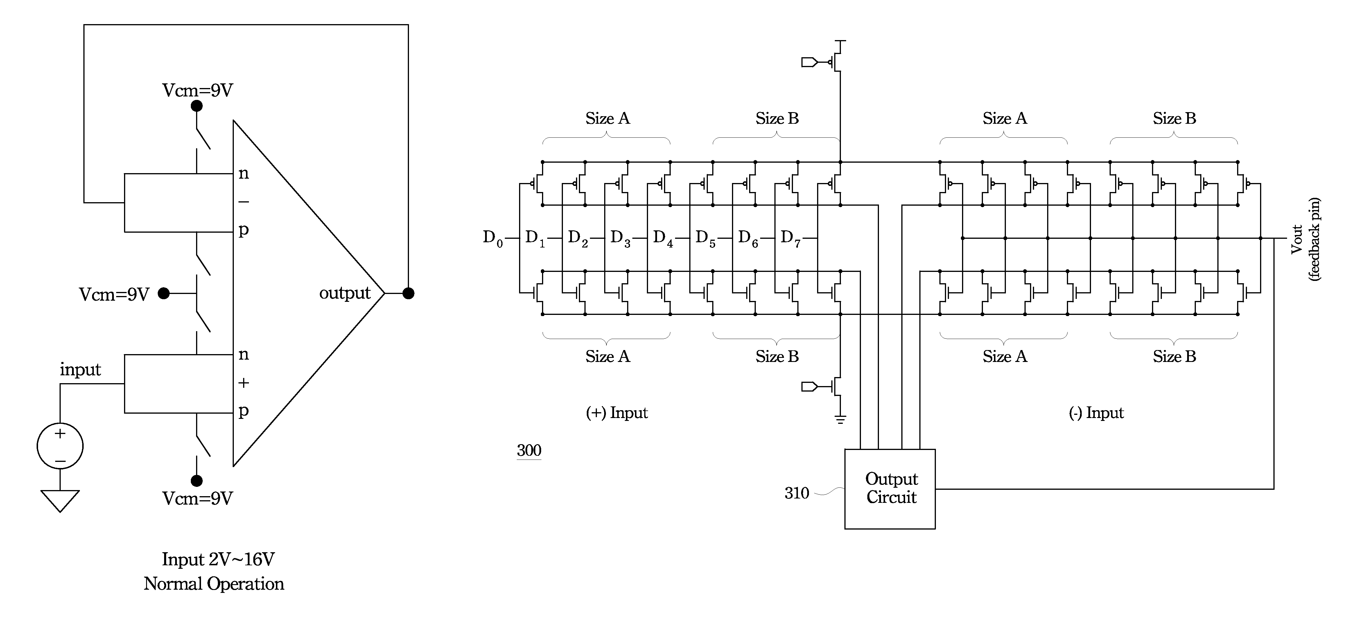
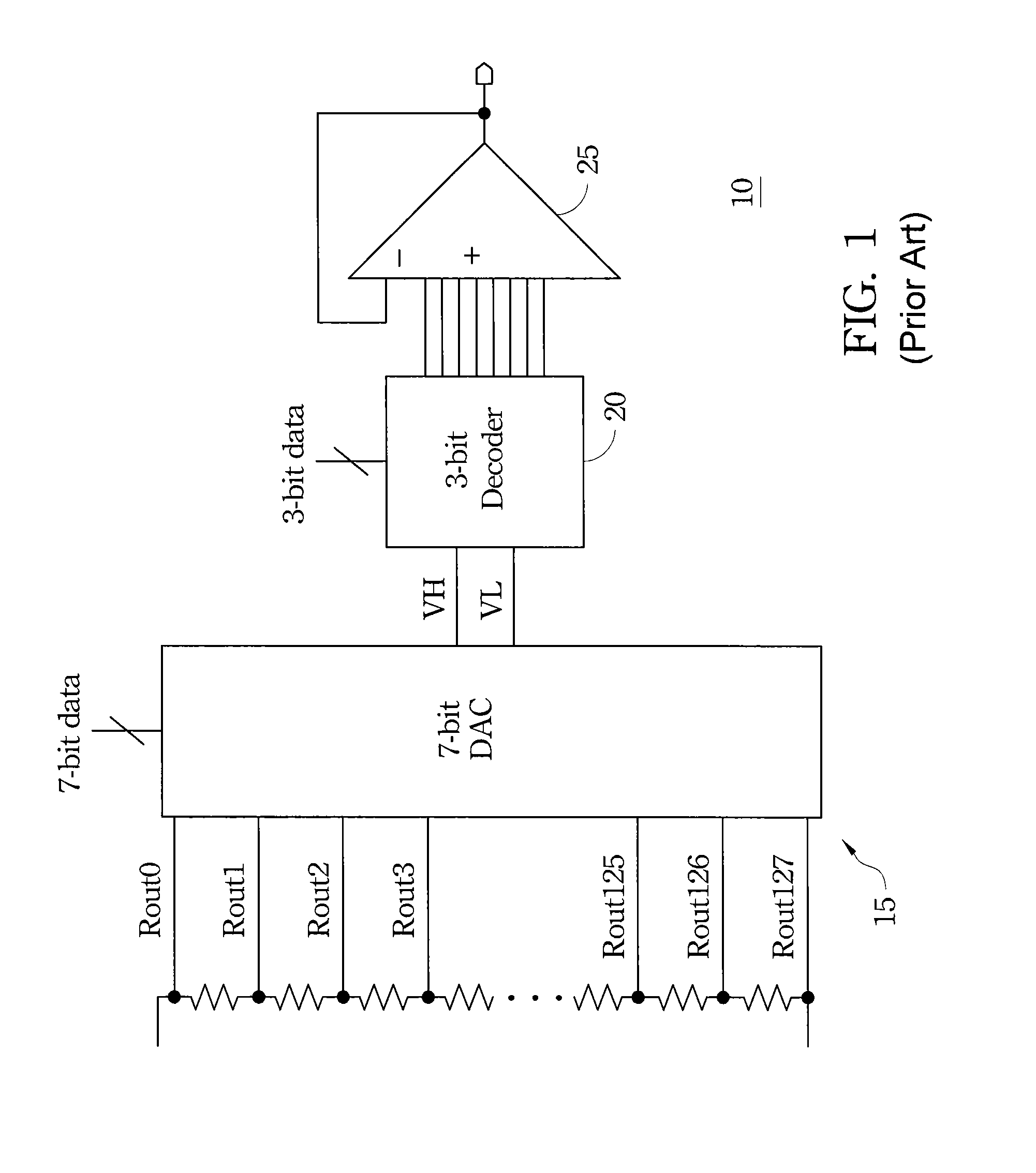
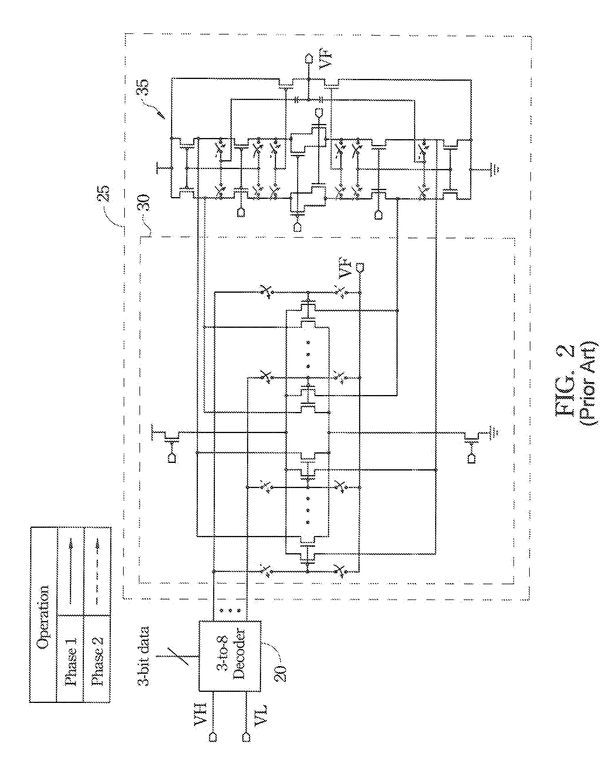
[0024]FIG. 1 is a diagram of a 10-bit driver 10 as described in Kang et al. and reprinted therefrom, the entirety of which is hereby incorporated by reference herein. To reduce the chip area consumed by the 10-bit driver, the 10-bit DAC required for the driver is split between a conventional 7-bit resistor-string DAC 15 and a unity-gain buffer, which has a 3-bit linear DAC built into the operational amplifier 25. The 7-bit resistor-string DAC 15 uses the 7 most significant bits of a 10-bit code to select two adjacent voltage l...


PUM


Abstract

A driver utilizes selective biasing of the terminal of an operational amplifier to reduce offset in the operational amplifier output. Each operational amplifier input includes a differential input pair of transistors including a NMOS transistor and PMOS transistor. At low and high ends of the input voltage range these transistors are selectively and individually coupled to either a standard input or biased to be on so as to contribute offset for offset compensation. The transistors are biased in a conventional manner for input voltages between the low and high ends of the voltage range.

Description

CROSS-REFERENCE TO RELATED APPLICATION[0001]This application is a non-provisional application of and claims priority to U.S. Provisional Patent Application No. 61 / 334,629 having the same title filed May 14, 2010, the entirety of which is hereby incorporated by reference herein.FIELD OF THE INVENTION[0002]The present invention relates to LCD drivers, and more particularly to LCD drivers utilizing digital-to-analog (DAC) converters.BACKGROUND OF THE INVENTION[0003]Today's advanced electronics, such as high definition televisions, place ever increasing demands on electronics. For example, customers demand HDTV display systems that can display images with more and more natural colors. Typical LCD drivers for driving pixel arrays of an LCD display use digital-to-analog converters to convert digital codes representing voltage levels to corresponding analog outputs. For example, sixteen binary numbers can be expressed using 4-bits to represent output voltages of the DAC. An actual analog o...

Claims


Application Information

Patent Timeline
Patent Type & Authority Patents(United States)
IPC IPC(8): G06G7/12
CPCG09G3/3688G09G2310/027G09G3/36H03F3/45H03M1/66
Inventor PENG, YUNG-CHOWCHOU, WEN-SHENCHANG, CHING-HOCHEN, WAN-TE
Owner TAIWAN SEMICON MFG CO LTD
Why Eureka
Try Eureka