Semiconductor device manufacturing method and plasma etching apparatus

a technology of plasma etching and semiconductor devices, which is applied in the direction of plasma technique, electric discharge tubes, decorative arts, etc., can solve the problems of difficult pattern formation, and achieve the effect of high selectivity and high accuracy

Active Publication Date: 2013-07-23
TOKYO ELECTRON LTD
View PDF4 Cites 207 Cited by
  • Summary
  • Abstract
  • Description
  • Claims
  • Application Information

AI Technical Summary

Benefits of technology

[0007]In view of the above, the present invention provides a semiconductor device manufacturing method and a plasma etching apparatus, capable of uniformly forming a fine pattern with high accuracy and high selectivity.

Problems solved by technology

However, due to the trade-off relationship between the selectivity and the pattern shape, it is difficult to form a pattern, e.g., a thin and deep hole, a line-and-space pattern having a small width and a tall height, or the like, with high selectivity.

Method used


Image

  • Semiconductor device manufacturing method and plasma etching apparatus
  • Semiconductor device manufacturing method and plasma etching apparatus
  • Semiconductor device manufacturing method and plasma etching apparatus

Examples


Embodiment Construction

[0019]Embodiments of the present invention will now be described with reference to the accompanying drawings which form a part hereof.

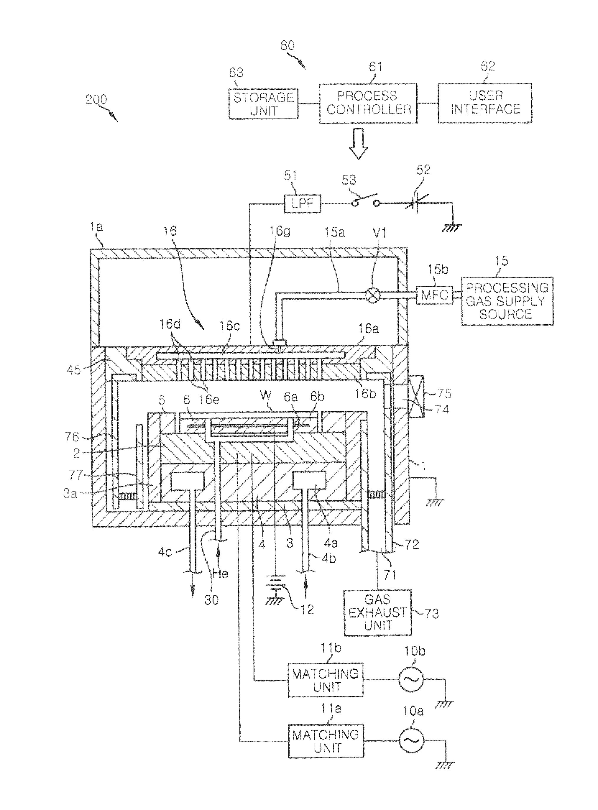
[0020]FIG. 1 schematically shows a configuration of a plasma etching apparatus 200 in accordance with an embodiment of the present invention. The plasma etching apparatus 200 includes a processing chamber 1 which is airtightly configured and electrically grounded. The processing chamber 1 has a cylindrical shape, and is made of, e.g., aluminum having an anodically oxidized surface.

[0021]Disposed in the processing chamber 1 is a mounting table 2 for supporting thereon a semiconductor wafer W as a target substrate horizontally. The mounting table 2 is made of, e.g., aluminum having an anodically oxidized surface, and serves as a lower electrode. The mounting table 2 is supported by a conductive support 4 via an insulating plate 3. Further, a focus ring 5 formed of, e.g., single-crystalline silicon, is disposed on an outer peripheral portion of a top sur...


PUM

PropertyMeasurementUnit
time periodaaaaaaaaaa
sizeaaaaaaaaaa

Abstract

A semiconductor device manufacturing method includes a plasma etching step for etching an etching target film formed on a substrate accommodated in a processing chamber. In the plasma etching step, a processing gas including a gaseous mixture containing predetermined gases is supplied into the processing chamber, and a cycle including a first step in which a flow rate of at least one of the predetermined gases is set to a first value during a first time period and a second step in which the flow rate thereof is set to a second value that is different from the first value during a second time period is repeated consecutively at least three times without removing a plasma. The first time period and the second time period are set to about 1 to 15 seconds.

Description

CROSS-REFERENCE TO RELATED APPLICATIONS[0001]This application claims priority to Japanese Patent Application No. 2010-024552 filed on Feb. 5, 2010 and U.S. Provisional Application No. 61 / 310,513 filed on Mar. 4, 2010, the entire contents of which are incorporated herein by reference.FIELD OF THE INVENTION[0002]The present invention relates to a semiconductor device manufacturing method and a plasma etching apparatus.BACKGROUND OF THE INVENTION[0003]A semiconductor device manufacturing process includes a process for plasma-etching various films formed on a substrate, e.g., a semiconductor wafer or the like, provided in a processing chamber of a plasma etching apparatus.[0004]In the plasma etching apparatus, the interior of the processing chamber accommodating therein a substrate, e.g., a semiconductor wafer or the like, is set to a depressurized atmosphere of a predetermined pressure and a predetermined processing gas is supplied into the processing chamber. The processing gas is con...

Claims


Application Information

Patent Timeline
Patent Type & Authority Patents(United States)
IPC IPC(8): C03C15/00
CPCH01J37/32091H01J37/32165H01J37/3244H01J37/32449H01L21/3065H01L21/31116H01L21/31122H01L21/32137H01L21/67069H01J37/32706H01L21/203H01L21/205H01L21/02H01L21/02266H01L21/302H01L21/30621H01L21/324H01L21/76825H01L21/76826H05H1/46
Inventor KUSHIBIKI, MASATONISHIMURA, EIICHI
Owner TOKYO ELECTRON LTD
Why Eureka
Try Eureka