Vertical polysilicon-germanium heterojunction bipolar transistor

a technology of bipolar transistor and polysilicon, which is applied in the direction of semiconductor devices, basic electric elements, electrical equipment, etc., can solve the problem of not being able to increase the ge concentration in the base region of sige alloy further, and achieve the effect of reducing the emitter-base bias

Active Publication Date: 2013-07-23
GLOBALFOUNDRIES US INC
View PDF19 Cites 9 Cited by
  • Summary
  • Abstract
  • Description
  • Claims
  • Application Information

AI Technical Summary

Benefits of technology

[0007]In the present disclosure, a vertical heterojunction bipolar transistor (HBT) includes doped polysilicon having a doping of a first conductivity type as a wide-gap-emitter with an energy bandgap of about 1.12 eV and doped single crystalline Ge having a doping of the second conductivity type as the base having an energy bandgap of about 0.66 eV. Doped single crystalline Ge having a doping of the first conductivity type is employed as the collector. Because the base and the collector include the same semiconductor material, i.e., Ge, having the same lattice constant, there is no lattice mismatch issue between the collector and the base. Further, because the emitter is polycrystalline and the base is single crystalline, there is no lattice mismatch issue between the base and the emitter. The small band gap of the base enables reduction of the emitter-base bias by a factor of about 2 compared to a regular silicon-base bipolar transistor.

Problems solved by technology

Further increase in the Ge concentration in the SiGe alloy in the base region is not possible because Ge concentration greater than 15% in a SiGe alloy destroys epitaxial alignment between the base and the collector due to excessive lattice mismatch between the underlying silicon material and the SiGe alloy.

Method used


Image

  • Vertical polysilicon-germanium heterojunction bipolar transistor
  • Vertical polysilicon-germanium heterojunction bipolar transistor
  • Vertical polysilicon-germanium heterojunction bipolar transistor

Examples


first embodiment

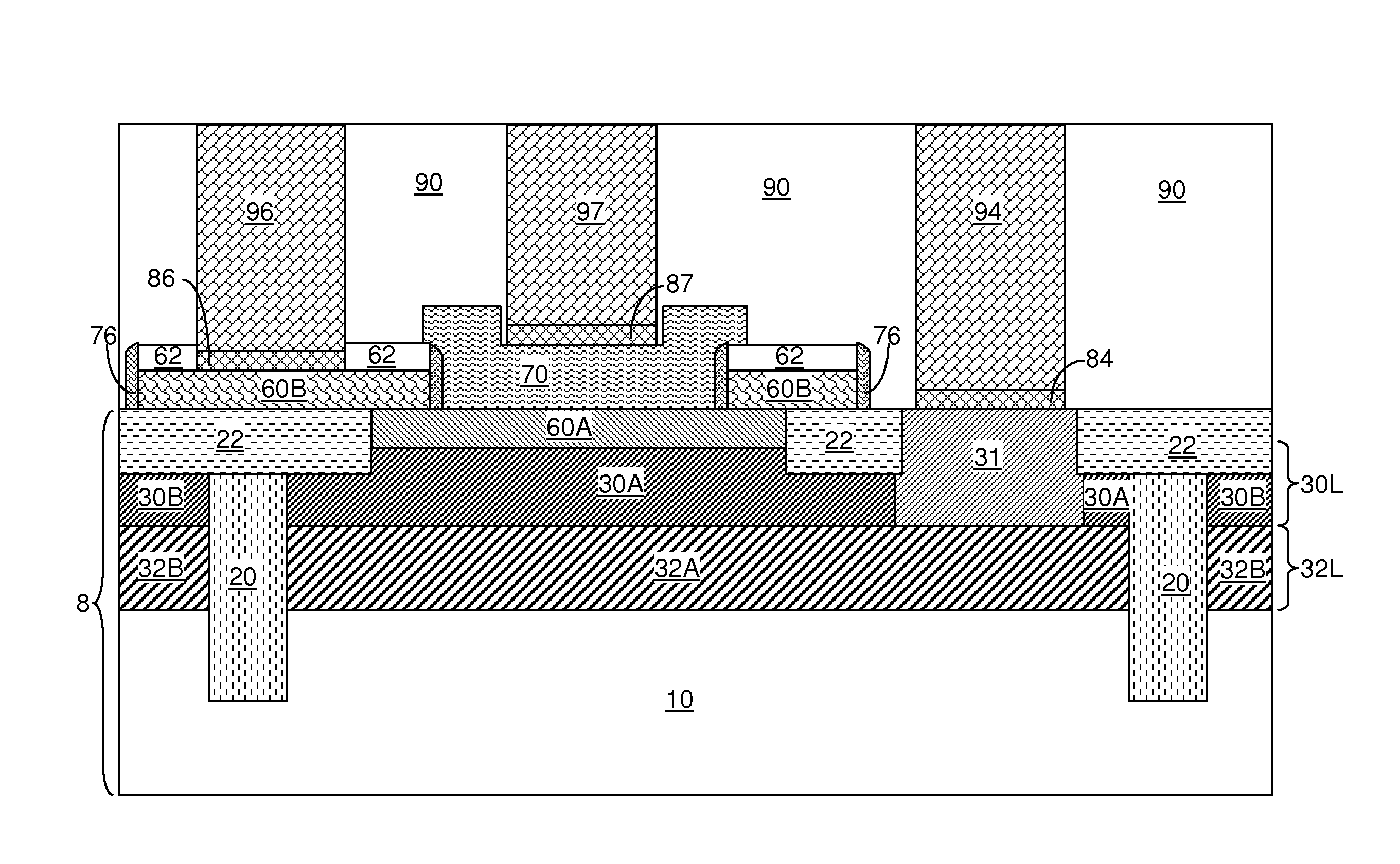
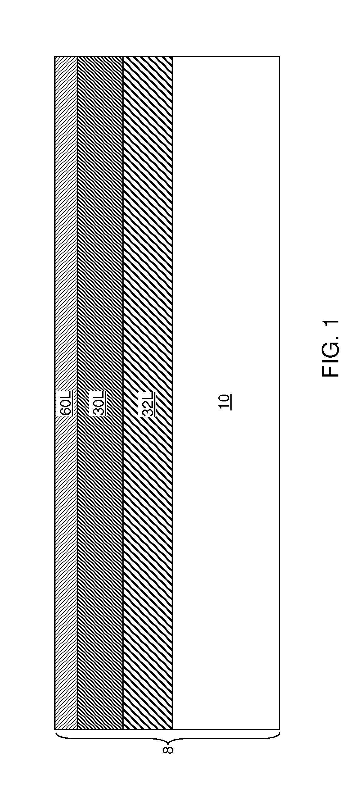
[0023]Referring to FIG. 1, a first exemplary structure according to the present disclosure includes a substrate 8, which includes a vertical stack, from bottom to top, of a substrate layer 10, a subcollector layer 32L, a collector layer 30L, and a base layer 60L. The entirety of the substrate 8 can be a single crystalline substrate with epitaxial alignment throughout the entirety thereof. The substrate 8 of FIG. 1 can be provided, for example, by providing a single crystalline germanium substrate and implanting dopants of various conductivity types into an upper portion of the single crystalline germanium substrate. For example, dopants of a first conductivity type, which can be p-type or n-type, can be implanted into the single crystalline germanium substrate to form the subcollector layer 32L and the collector layer 30L. Typically, the single crystalline germanium substrate is intrinsic or has a doping of the opposite conductivity type to the first conductivity type, which is here...

third embodiment

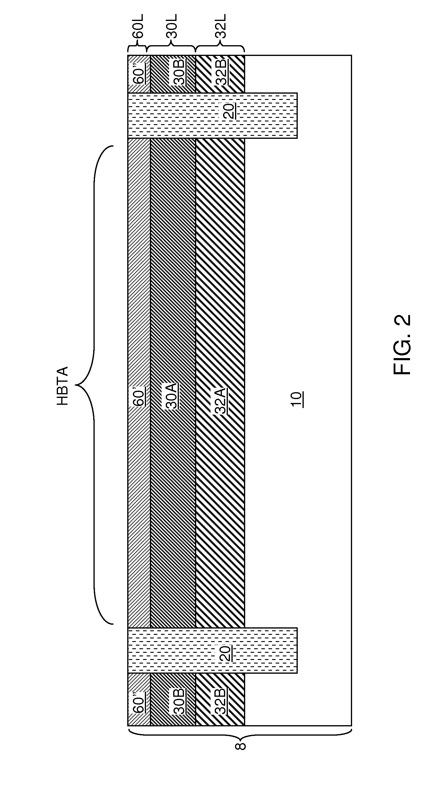
[0053]Referring to FIG. 11, a third exemplary structure according to the present disclosure is derived from the second exemplary structure by omitting the formation of a subcollector layer 32L at the processing step corresponding to the processing step of FIG. 1. Thus, the bottom surface of the collector 30A contacts the top surface of a buried insulator layer 12 within the GOI substrate 8′. The HBT structure in the third exemplary structure can provide the same functional advantage as the HBT structure in the first exemplary structure in addition to providing enhanced electrical isolation from adjacent devices and the substrate layer 10 due to the presence of the buried insulator layer 12. The HBT structure in the third exemplary structure simplifies the manufacturing process by eliminating the subcollector 32A, but the resistance between the collector contact via structure 94 and the collector 30A can be greater in the third exemplary structure than in the second exemplary structu...


PUM


Abstract

A vertical heterojunction bipolar transistor (HBT) includes doped polysilicon having a doping of a first conductivity type as a wide-gap-emitter with an energy bandgap of about 1.12 eV and doped single crystalline Ge having a doping of the second conductivity type as the base having the energy bandgap of about 0.66 eV. Doped single crystalline Ge having of doping of the first conductivity type is employed as the collector. Because the base and the collector include the same semiconductor material, i.e., Ge, having the same lattice constant, there is no lattice mismatch issue between the collector and the base. Further, because the emitter is polycrystalline and the base is single crystalline, there is no lattice mismatch issue between the base and the emitter.

Description

RELATED APPLICATIONS[0001]The present application is related to co-assigned and co-pending U.S. application Ser. No. 13 / 048,342.BACKGROUND[0002]The present disclosure relates to semiconductor devices, and particularly to vertical polysilicon-germanium heterojunction bipolar transistors and methods of manufacturing the same.[0003]The collector current of a bipolar transistor is a function of the energy bandgap of the base region material. For a regular silicon base bipolar transistor, it takes an emitter-base bias of about 0.92 V to obtain a collector current density of 10 mA / μm2. It is desirable to be able to reduce the voltage needed to drive a bipolar transistor.[0004]The state of art SiGe-base bipolar transistors have silicon in the collector, a SiGe alloy in the base, and polysilicon as emitter. The distribution of Ge across the SiGe base region can be relatively uniform, or can be graded with higher Ge concentration near the collector end and lower, or zero, Ge concentration at...

Claims


Application Information

Patent Timeline
Patent Type & Authority Patents(United States)
IPC IPC(8): H01L29/66
CPCH01L29/737H01L29/7375H01L21/76229H01L29/66242H01L29/0649H01L29/0821H01L29/165
Inventor CAI, JINCHAN, KEVIN K.HAENSCH, WILFRIED E.NING, TAK H.
Owner GLOBALFOUNDRIES US INC
Why Eureka
Try Eureka