Horizontal polysilicon-germanium heterojunction bipolar transistor

a technology of polysilicongermanium and heterojunction, which is applied in the direction of semiconductor devices, basic electric elements, electrical equipment, etc., can solve the problem of not being able to increase the ge concentration in the base region of sige alloy further, and achieve the effect of reducing the emitter-base bias

Active Publication Date: 2012-09-20
AURIGA INNOVATIONS INC
View PDF9 Cites 14 Cited by
  • Summary
  • Abstract
  • Description
  • Claims
  • Application Information

AI Technical Summary

Benefits of technology

[0007]In the present disclosure, a horizontal heterojunction bipolar transistor (HBT) includes doped single crystalline Ge having a doping of the first conductivity type as the base having an energy bandgap of about 0.66 eV, and doped polysilicon having a doping of a second conductivity type as a wide-gap-emitter having an energy bandgap of about 1.12 eV. In one embodiment, doped polysilicon having a doping of the second conductivity type is employed as the collector. In other embodiments, a single crystalline Ge having a doping of the second conductivity type is employed as the collector. In such embodiments, because the base and the collector include the same semiconductor material, i.e., Ge, having the same lattice constant, there is no lattice mismatch issue between the collector and the base. In both embodiments, because the emitter is polycrystalline and the base is single crystalline, there is no lattice mismatch issue between the base and the emitter. The small band gap of the base enables reduction of the emitter-base bias by a factor of about 2 compared to a regular silicon-base bipolar transistor.

Problems solved by technology

Further increase in the Ge concentration in the SiGe alloy in the base region is not possible because Ge concentration greater than 15% in a SiGe alloy destroys epitaxial alignment between the base and the collector due to excessive lattice mismatch between the underlying silicon material and the SiGe alloy.

Method used


Image

  • Horizontal polysilicon-germanium heterojunction bipolar transistor
  • Horizontal polysilicon-germanium heterojunction bipolar transistor
  • Horizontal polysilicon-germanium heterojunction bipolar transistor

Examples


first embodiment

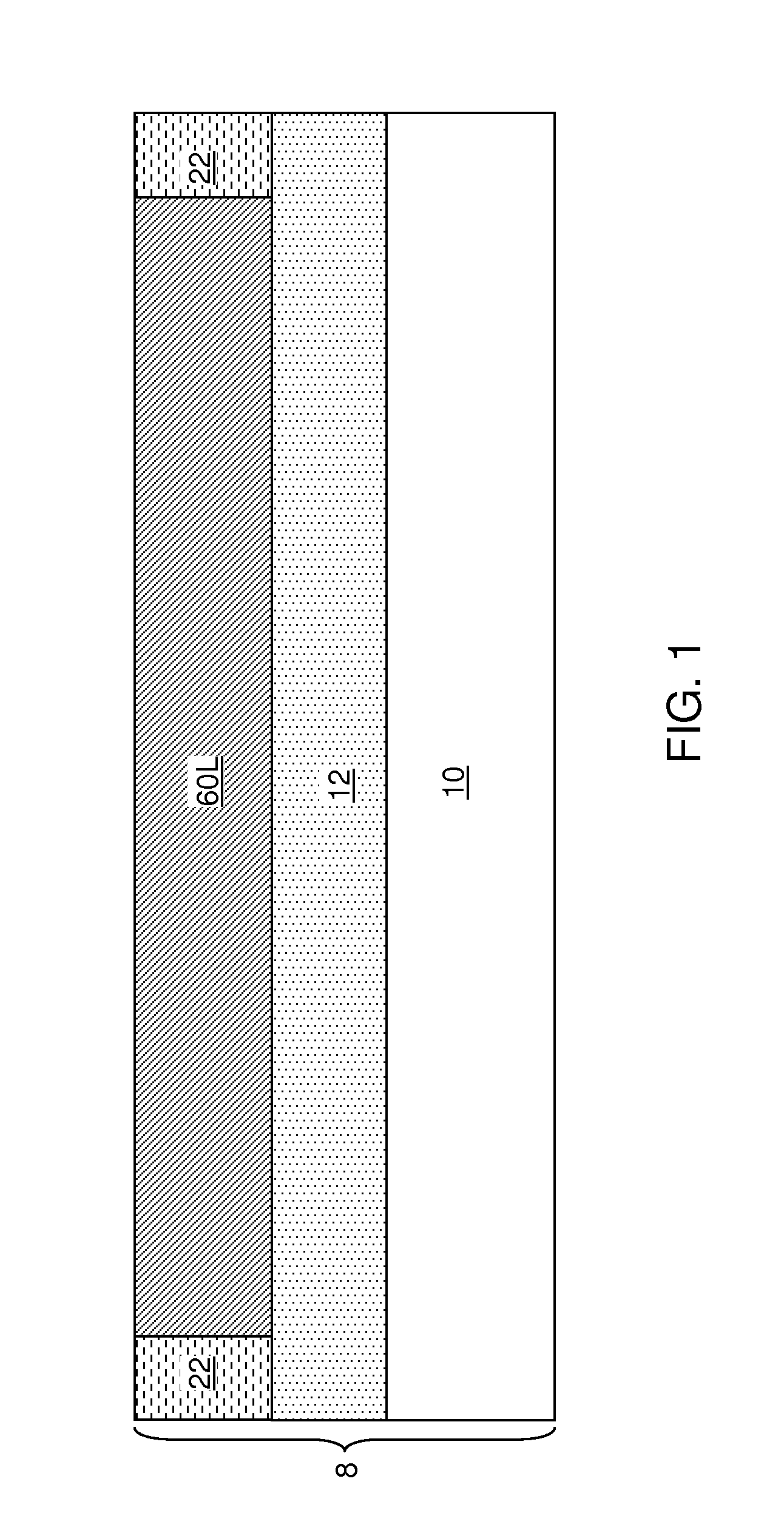
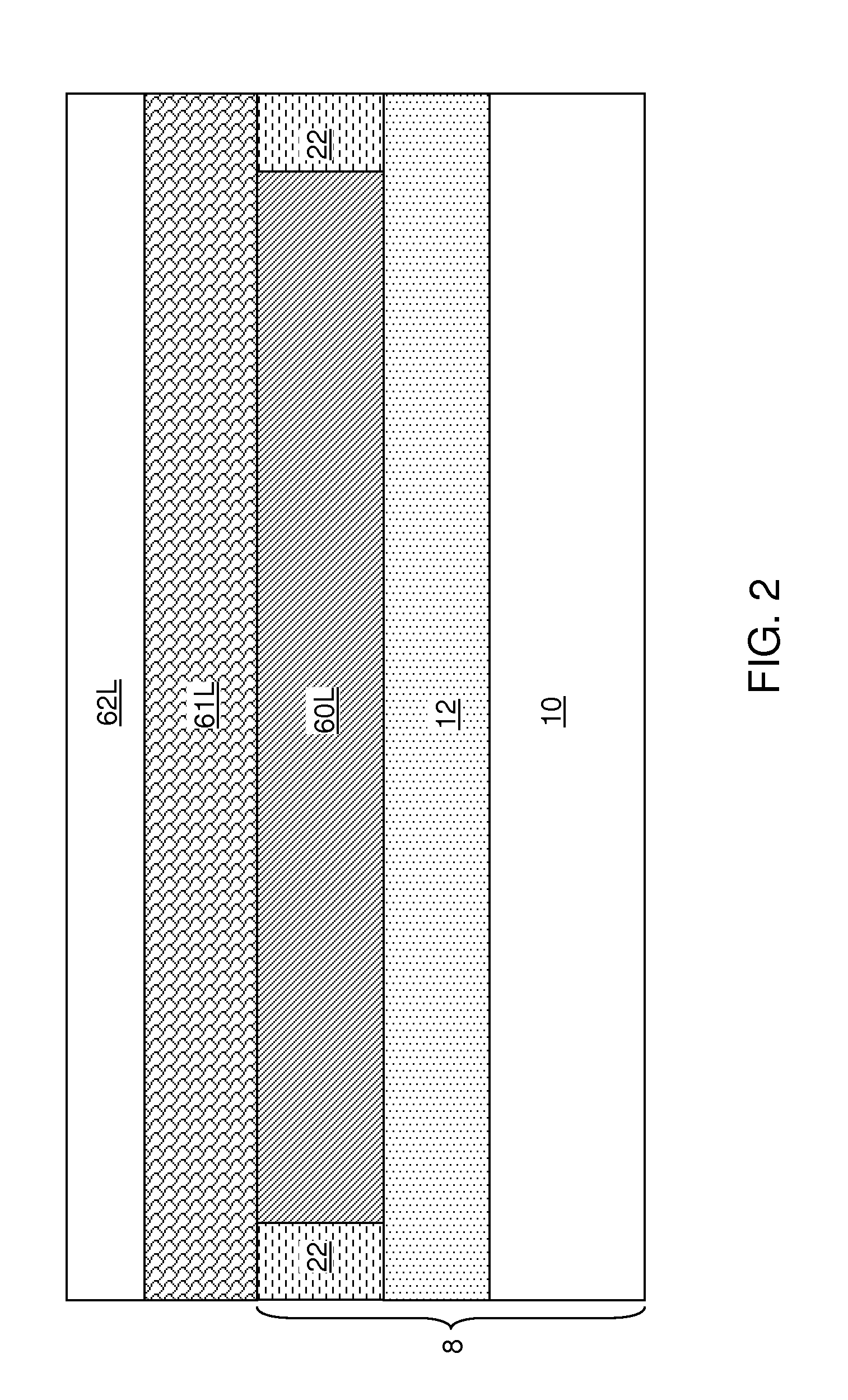
[0031]Referring to FIG. 1, a first exemplary structure according to the present disclosure includes a germanium-on-insulator (GOI) substrate 8. The GOI substrate includes a handle substrate 10, a buried insulator layer 12, and a top germanium layer 60L having single crystalline germanium. The handle substrate 10 can include a semiconductor material, a dielectric material, and / or a conductive material. If the handle substrate 10 includes a semiconductor material, the handle substrate 10 can be a single crystalline silicon layer, a polysilicon layer, a single crystalline germanium layer, a polycrystalline germanium layer, a single crystalline silicon-germanium alloy layer, a polysilicon-germanium alloy layer, or a combination thereof.

[0032]The buried insulator layer 12 includes a dielectric material such as silicon oxide, silicon nitride, silicon oxynitride, germanium oxide, germanium nitride, germanium oxynitride, or a combination thereof. The thickness of the buried insulator layer ...

third embodiment

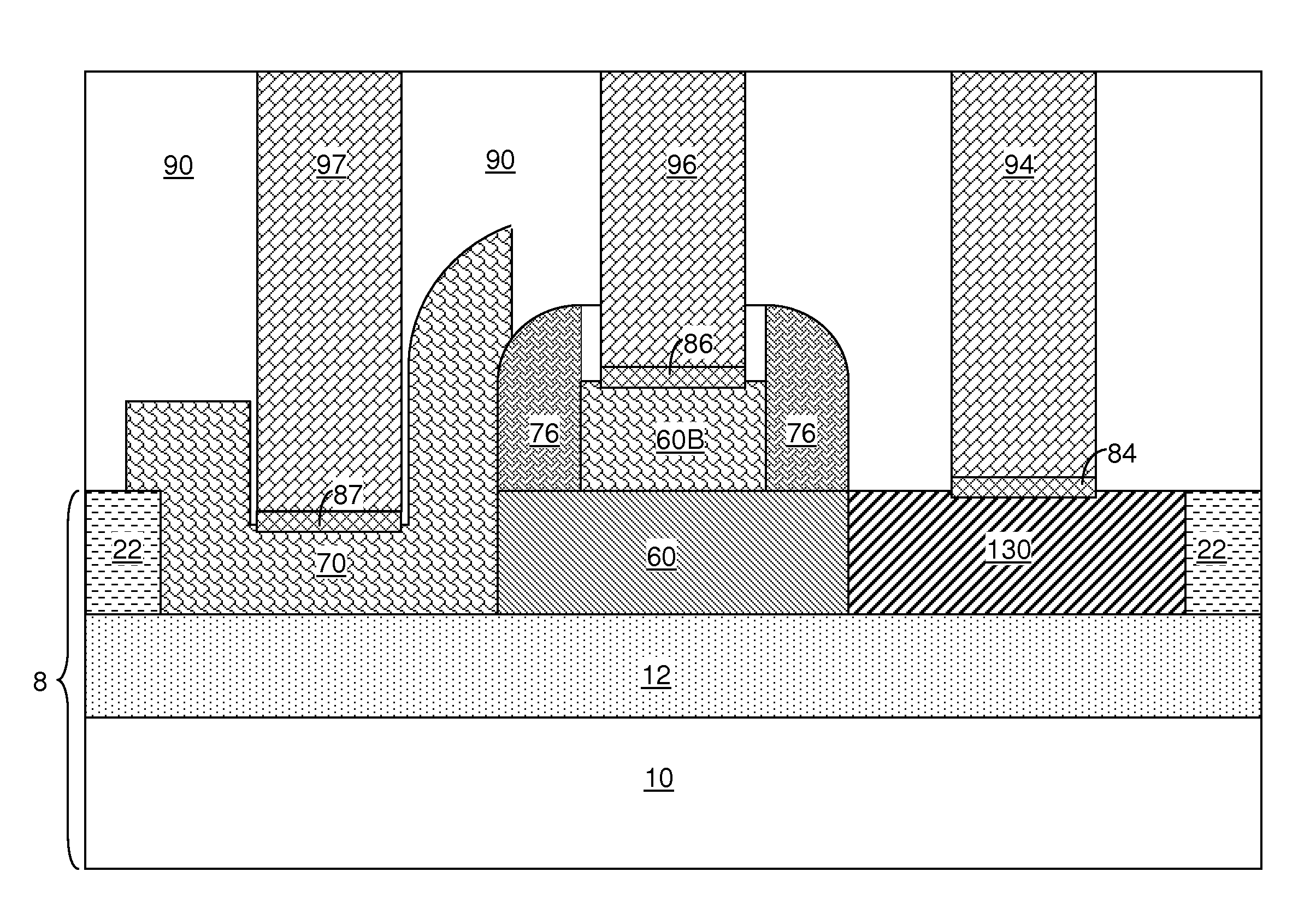
[0064]Referring to FIG. 15, a third exemplary structure according to the present disclosure is derived from the second exemplary structure of FIG. 8 by forming an emitter-side trench 69 employing the same processing step as in FIG. 10 without forming a dielectric masking layer 140 illustrated in FIGS. 9 and 10. Thus, a photoresist (not shown) can be applied over the second exemplary structure of FIG. 8 and lithographically patterned to form an opening in the emitter side area ESA. The periphery of the opening in the photoresist can overlie the extrinsic base cap 62 and the portion of the shallow trench isolation structure 22 around the emitter side area ESA. The disposable emitter-side structure 71 is etched to form an emitter-side trench 69 as illustrated in FIG. 10. However, a dielectric masking layer of FIG. 10 is not present in the third exemplary structure at this step.

second embodiment

[0065]A doped polysilicon layer 70L having the same composition and thickness as in the second embodiment can be deposited employing the same deposition methods. The doped polysilicon layer 70L can be formed over the extrinsic base cap 62, the dielectric spacer 76, the collector 130, and the shallow trench isolation structure 22 and within the emitter-side trench 69 as a conformal layer having substantially the same thickness on vertical portions and horizontal portions. The doped polysilicon layer 70L has a doping of the second conductivity type.

[0066]Referring to FIG. 16, the doped polysilicon layer 70L is lithographically patterned, for example, by applying a photoresist (not shown), lithographically patterning the photoresist, and transferring the pattern in the photoresist in the underlying doped polysilicon layer 70L by an etch that employs the photoresist as an etch mask. The photoresist is subsequently removed. A first remaining portion of the doped polysilicon layer 70L for...


PUM


Abstract

A horizontal heterojunction bipolar transistor (HBT) includes doped single crystalline Ge having a doping of the first conductivity type as the base having an energy bandgap of about 0.66 eV, and doped polysilicon having a doping of a second conductivity type as a wide-gap-emitter having an energy bandgap of about 1.12 eV. In one embodiment, doped polysilicon having a doping of the second conductivity type is employed as the collector. In other embodiments, a single crystalline Ge having a doping of the second conductivity type is employed as the collector. In such embodiments, because the base and the collector include the same semiconductor material, i.e., Ge, having the same lattice constant, there is no lattice mismatch issue between the collector and the base. In both embodiments, because the emitter is polycrystalline and the base is single crystalline, there is no lattice mismatch issue between the base and the emitter.

Description

RELATED APPLICATIONS[0001]The present application is related to co-assigned and co-pending U.S. application Ser. No. ______ (Attorney Docket No: YOR920100658US1; SSMP 27108).BACKGROUND[0002]The present disclosure relates to semiconductor devices, and particularly to horizontal polysilicon-germanium heterojunction bipolar transistors and methods of manufacturing the same.[0003]The collector current of a bipolar transistor is a function of the energy bandgap of the base region material. For a regular silicon base bipolar transistor, it takes an emitter-base bias of about 0.92 V to obtain a collector current density of 10 mA / μm2. It is desirable to be able to reduce the voltage needed to drive a bipolar transistor.[0004]The state of art SiGe-base bipolar transistors have silicon in the collector, a SiGe alloy in the base, and polysilicon as emitter. The distribution of Ge across the SiGe base region can be relatively uniform, or can be graded with higher Ge concentration near the colle...

Claims


Application Information

Patent Timeline
Patent Type & Authority Applications(United States)
IPC IPC(8): H01L29/737H01L21/331
CPCH01L29/0808H01L29/0821H01L29/737H01L29/66265H01L29/66242
Inventor CAI, JINCHAN, KEVIN K.HAENSCH, WILFRIED W.NING, TAK H.
Owner AURIGA INNOVATIONS INC
Why Eureka
Try Eureka