Manufacturing method of electronic device package, electronic device package, and oscillator

a manufacturing method and electronic device technology, applied in semiconductor devices, transducer details, semiconductor/solid-state device details, etc., can solve problems such as difficulty in identifying product identification numbers on the cover substrate, and achieve the effect of suppressing the warping of the cover substra

Active Publication Date: 2013-09-10
SEIKO INSTR INC
View PDF11 Cites 3 Cited by
  • Summary
  • Abstract
  • Description
  • Claims
  • Application Information

AI Technical Summary

Benefits of technology

[0013]The invention was devised in view of the foregoing and has an object to provide an electronic device package in which a base substrate and a cover substrate are bonded together via a metal film in a stable manner by minimizing warping of the substrate even when the substrate whose one surface and other surface have different shapes is made thinner.
[0015]According to the manufacturing method of the electronic device package of the invention, the metal film is also formed on the cover substrate on the surface opposite to the surface in which the concave portions are formed. Accordingly, even when the cover substrate becomes extremely thin, this metal film plays a role of preventing warping of the cover substrate. Hence, there can be achieved an advantage that warping of the cover substrate can be suppressed to the least extent when the base substrate and the cover substrate are bonded together. Further, because the metal film is formed on the cover substrate on the surface opposite to the surface bonded to the base substrate, there can be achieved another advantage that a product identification number can be inscribed on this metal film. In a case where the cover substrate is an insulator, it has been quite difficult to inscribe the product identification number on the cover substrate on the surface opposite to the surface bonded to the base substrate.

Problems solved by technology

In a case where the cover substrate is an insulator, it has been quite difficult to inscribe the product identification number on the cover substrate on the surface opposite to the surface bonded to the base substrate.

Method used


Image

  • Manufacturing method of electronic device package, electronic device package, and oscillator
  • Manufacturing method of electronic device package, electronic device package, and oscillator
  • Manufacturing method of electronic device package, electronic device package, and oscillator

Examples


Embodiment Construction

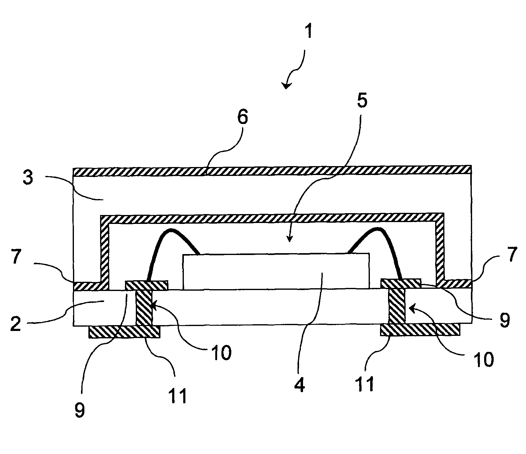
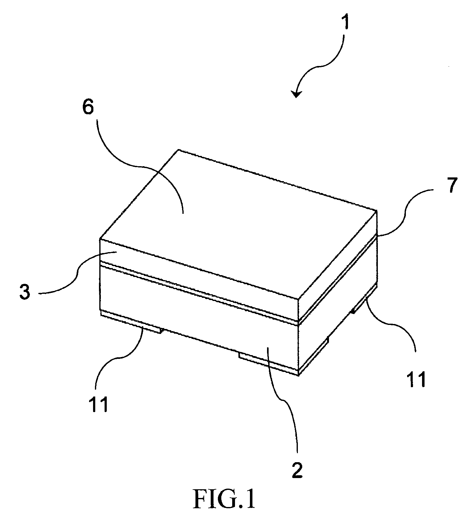
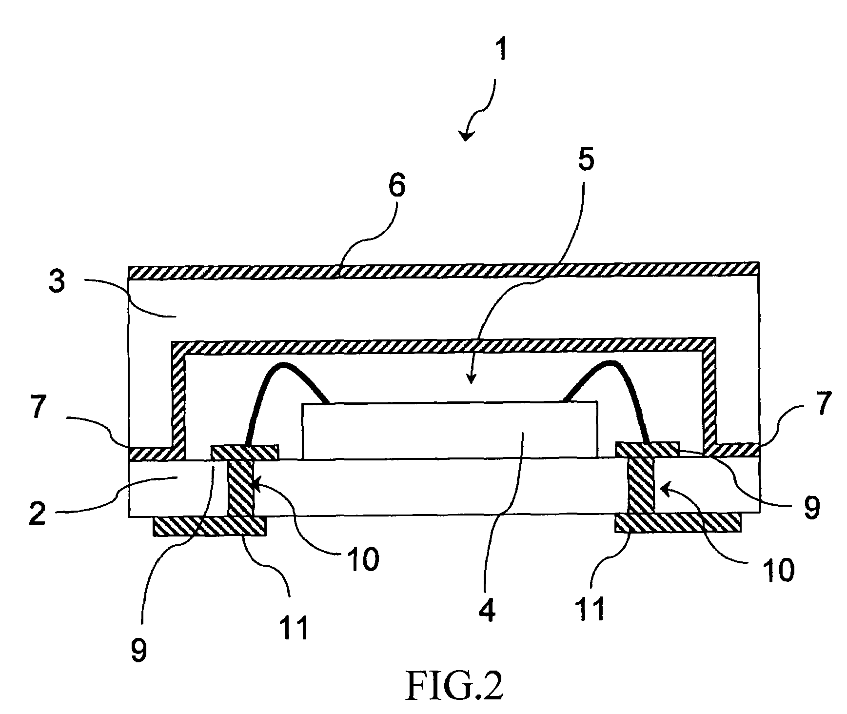
[0023]Hereinafter, one embodiment of the invention will be described with reference to FIG. 1 through FIG. 5B. As are shown in FIG. 1 and FIG. 2, an electronic device package 1 of this embodiment is a surface mount device package including a base substrate 2 and a cover substrate 3 laminated in two layers in a box shape and an electronic device 4 accommodated in a cavity 5 formed inside the box. The electronic device 4 means an LSI, an MEMS, a sensor, and a piezoelectric transducer, or a complex thereof.

[0024]Both the base substrate 2 and the cover substrate 3 are formed of an insulator, a semiconductor, metal, or a combination thereof and both are an insulator made, for example, of soda glass in this embodiment. In the case shown in FIG. 1 and FIG. 2, a rectangular concave portion that later forms a cavity 5 in which to accommodate the electronic device 4 is formed in the cover substrate 3 on the surface to which the base substrate 2 is bonded and the base substrate 2 is formed in ...


PUM

PropertyMeasurementUnit
thicknessaaaaaaaaaa
thicknessaaaaaaaaaa
thicknessaaaaaaaaaa

Abstract

A manufacturing method of an electronic device package includes: forming concave portions that later form the cavities in one surface of a cover substrate; forming a first metal film on the cover substrate on a surface opposite to the surface in which the concave portions are formed; forming a second metal film on the cover substrate on the surface in which the concave portions are formed; bonding a base substrate and the cover substrate together via the second metal film. It thus becomes possible to provide an electronic device package in which the base substrate and the cover substrate are boned together via the metal film in a stable manner by minimizing warping of the substrate even when the substrate is made thinner.

Description

RELATED APPLICATIONS[0001]This application claims priority under 35 U.S.C. §119 to Japanese Patent Application No. 2010-073340 filed on Mar. 26, 2010, the entire content of which is hereby incorporated by reference.BACKGROUND OF THE INVENTION[0002]1. Field of the Invention[0003]The present invention relates to a package for a surface mount device (SMD) in which an electronic device is encapsulated in a cavity formed between two substrates bonded together, and more particularly, to a structure to bond two substrates.[0004]2. Background Art[0005]Recently, electronic devices using a compact surface mount device package are employed often in mobile phones and personal digital assistants. Of these electronic devices, many components, such as a transducer, an MEMS, a gyrosensor, and an acceleration sensor, require a package of a hollow cavity structure. A structure in which a base substrate and a cover substrate are boned together via a metal film is known as a package of the hollow cavit...

Claims


Application Information

Patent Timeline
Patent Type & Authority Patents(United States)
IPC IPC(8): H01L29/84
CPCH01L21/50H03H9/1014H01L24/97H01L23/10H03H9/1071H01L2224/32225H01L2224/48227H01L2224/73265H01L2224/97H01L2924/01322H01L2224/48091H01L2924/1461H01L2924/15787H01L2924/00012H01L2224/85H01L2924/00H01L2924/00014H01L24/73H01L2924/14H01L2924/16152H01L23/043
Inventor YOSHIDA, YOSHIFUMI
Owner SEIKO INSTR INC
Why Eureka
Try Eureka