Electrically conductive pins for microcircuit tester

a microcircuit tester and electrically conductive pin technology, applied in the direction of emergency connections, coupling device connections, instruments, etc., can solve the problems of affecting the test results

Active Publication Date: 2013-09-17
JOHNSTECH INT
View PDF60 Cites 47 Cited by
  • Summary
  • Abstract
  • Description
  • Claims
  • Application Information

AI Technical Summary

Benefits of technology

[0004]The present invention is directed to equipment for testing microcircuits.
[0006]As microcircuits continually evolve to be smaller and more complex, the test equipment that tests the microcircuits also evolves. There is an ongoing effort to improve microcircuit test equipment, with improvements leading to an increase in reliability, an increase in throughput, and / or a decrease in expense.

Problems solved by technology

As microcircuits continually evolve to be smaller and more complex, the test equipment that tests the microcircuits also evolves.
Mounting a defective microcircuit on a circuit board is relatively costly.
Once mounted on a circuit board, removing a microcircuit is problematic because the very act of melting the solder for a second time ruins the circuit board.
Thus, if the microcircuit is defective, the circuit board itself is probably ruined as well, meaning that the entire value added to the circuit board at that point is lost.
Each microcircuit must be tested in a way that identifies all defective devices, but yet does not improperly identify good devices as defective.
Either kind of error, if frequent, adds substantial overall cost to the circuit board manufacturing process, and can add retest costs for devices improperly identified as defective devices.
Microcircuit test equipment itself is quite complex.
Because of the small size of microcircuit contacts and the spacings between them, even small errors in making the contact will result in incorrect connections.
Connections to the microcircuit that are misaligned or otherwise incorrect will cause the test equipment to identify the device under test (DUT) as defective, even though the reason for the failure is the defective electrical connection between the test equipment and the DUT rather than defects in the DUT itself.
A further problem in microcircuit test equipment arises in automated testing.
The sheer number of tests cause wear on the tester contacts making electrical connections to the microcircuit terminals during testing.
This wear dislodges conductive debris from both the tester contacts and the DUT terminals that contaminates the testing equipment and the DUTs themselves.
The debris eventually results in poor electrical connections during testing and false indications that the DUT is defective.
The debris adhering to the microcircuits may result in faulty assembly unless the debris is removed from the microcircuits.
Removing debris adds cost and introduces another source of defects in the microcircuits themselves.
If the test equipment is off line for extended periods of normal maintenance, the cost of testing an individual microcircuit increases.
In general, it is impractical to solder and remove each electrical terminal on the microcircuit being contacted by a corresponding electrical probe on the testbed.
After testing, when the device under test is released, the terminals separate from the pins and the circuits are broken.
First, in making the temporary contact with the ball terminals, the tester should not damage the S&P terminal surfaces that contact the circuit board, since such damage may affect the reliability of the solder joint for that terminal.
Tin-based solder alloys are likely to develop an oxide film on the outer surface that conducts poorly.

Method used


Image

  • Electrically conductive pins for microcircuit tester
  • Electrically conductive pins for microcircuit tester
  • Electrically conductive pins for microcircuit tester

Examples


Embodiment Construction

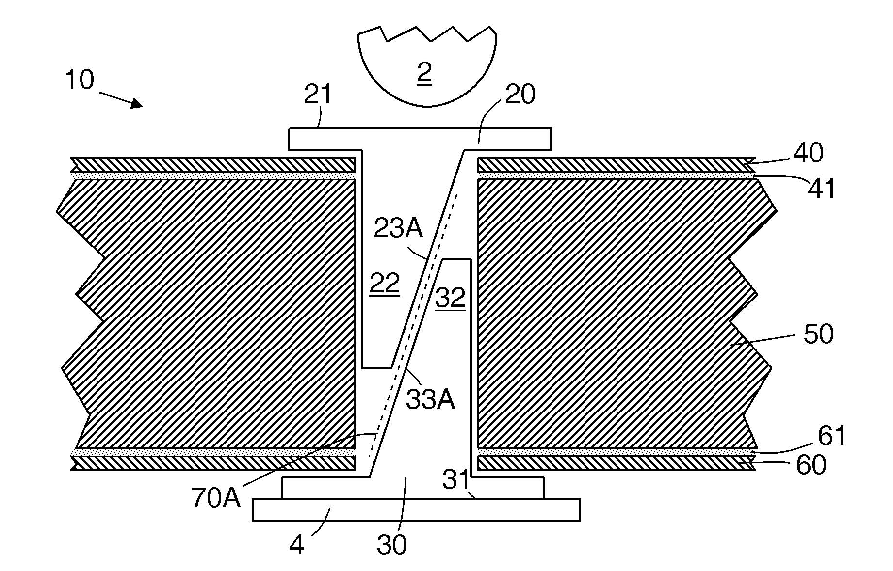
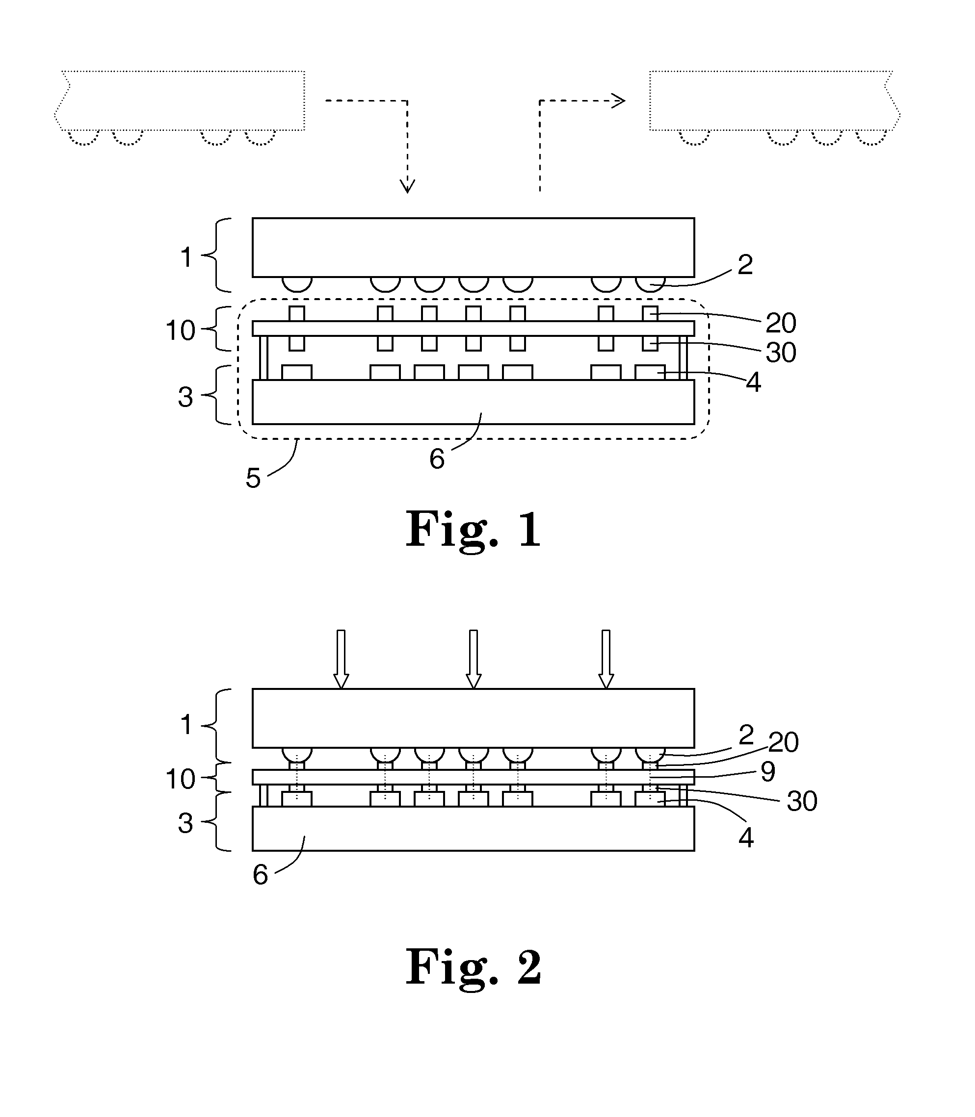
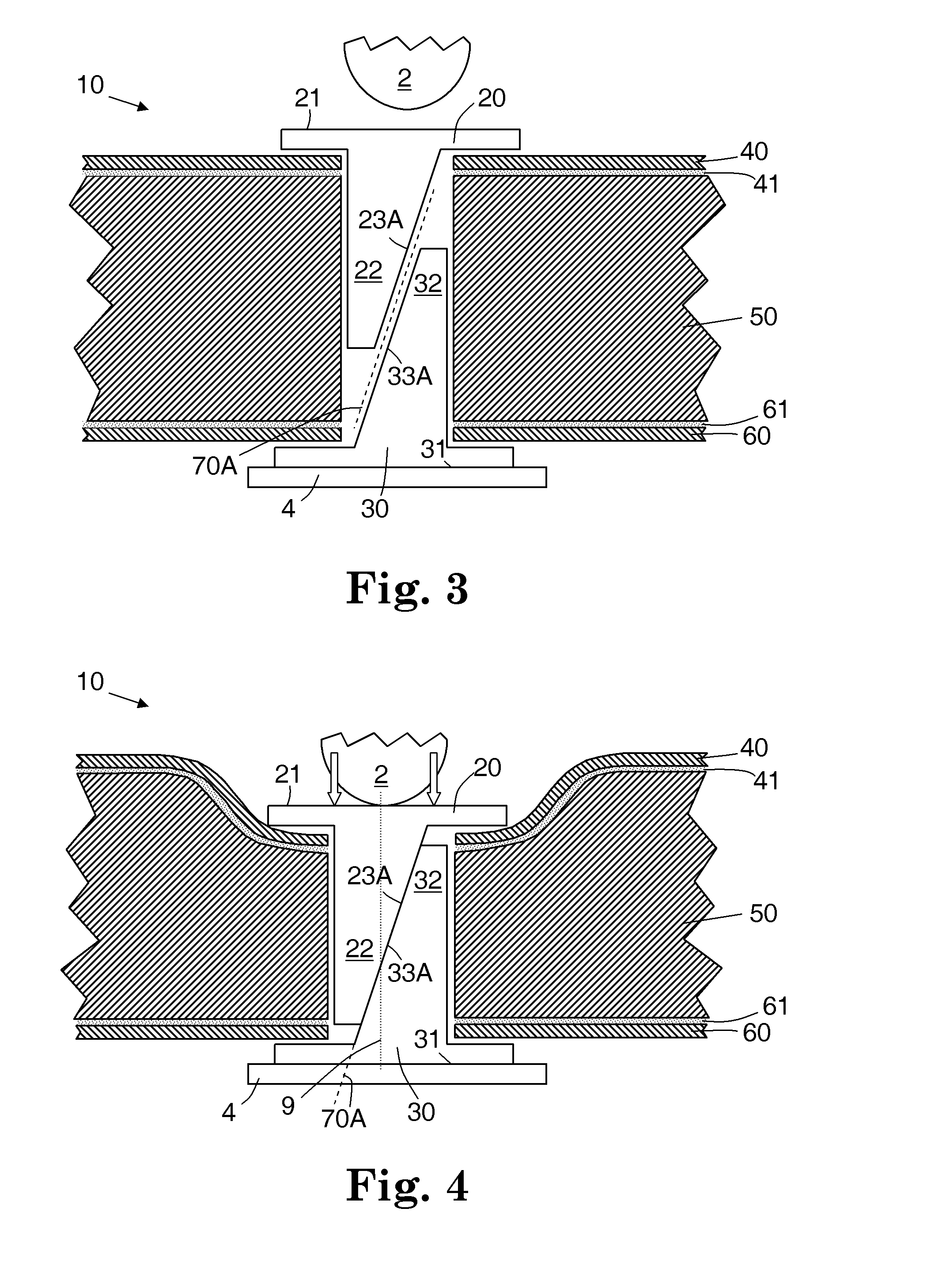
[0085]Consider an electrical chip that is manufactured to be incorporated into a larger system. When in use, the chip electrically connects the device to the larger system by a series of pins or terminals. For instance, the pins on the electrical chip may plug into corresponding sockets in a computer, so that the computer circuitry may electrically connect with the chip circuitry in a predetermined manner. An example of such a chip may be a memory card or processor for a computer, each of which may be insertable into a particular slot or socket that makes one or more electrical connections with the chip.

[0086]It is highly desirable to test these chips before they are shipped, or before they are installed into other systems. Such component-level testing may help diagnose problems in the manufacturing process, and may help improve system-level yields for systems that incorporate the chips. Therefore, sophisticated test systems have been developed to ensure that the circuitry in the ch...


PUM


Abstract

The terminals of a device under test are temporarily electrically connected to corresponding contact pads on a load board by a series of electrically conductive pin pairs. The pin pairs are held in place by an interposer membrane that includes a top contact plate facing the device under test, a bottom contact plate facing the load board, and a vertically resilient, non-conductive member between the top and bottom contact plates. Each pin pair includes a top and bottom pin, which extend beyond the top and bottom contact plates, respectively, toward the device under test and the load board, respectively. The top and bottom pins contact each other at an interface that is inclined with respect to the membrane surface normal. When compressed longitudinally, the pins translate toward each other by sliding along the interface. The sliding is largely longitudinal, with a small and desirable lateral component determined by the inclination of the interface.

Description

CROSS-REFERENCE TO RELATED APPLICATIONS[0001]This application claims priority of provisional application No. 61 / 158,934, filed on Mar. 10, 2009 and provisional application No. 61 / 307,100, filed on Feb. 23, 2010, which hereby is incorporated herein by reference in its entirety.STATEMENT REGARDING FEDERALLY SPONSORED RESEARCH OR DEVELOPMENT[0002]Not ApplicableBACKGROUND OF THE INVENTION[0003]1. Field of the Invention[0004]The present invention is directed to equipment for testing microcircuits.[0005]2. Description of the Related Art[0006]As microcircuits continually evolve to be smaller and more complex, the test equipment that tests the microcircuits also evolves. There is an ongoing effort to improve microcircuit test equipment, with improvements leading to an increase in reliability, an increase in throughput, and / or a decrease in expense.[0007]Mounting a defective microcircuit on a circuit board is relatively costly. Installation usually involves soldering the microcircuit onto th...

Claims


Application Information

Patent Timeline
Patent Type & Authority Patents(United States)
IPC IPC(8): G01R31/20G01R31/00
CPCG01R1/0466H01R13/2414G01R1/0416G01R1/0483H01H13/702H01H2203/04H01R12/7082H01H2207/028H01H2209/052H01H2205/006G01R1/0735G01R1/07371G01R1/06733G01R31/28
Inventor NELSON, JOHN E.SHERRY, JEFFREY C.ALLADIO, PATRICK J.OBERG, RUSSELL F.WARWICK, BRIANMICHALKO, GARY W.
Owner JOHNSTECH INT
Why Eureka
Try Eureka