Structure and method for reducing EM radiation, and electric object and manufacturing method thereof

a technology of em radiation and structure, applied in the direction of waveguides, line-transmission details, high-frequency circuit adaptations, etc., can solve the problems of reducing the effect of em radiation, affecting the quality of signal, and unable to avoid the asymmetry between two signal lines, so as to reduce the influence of em radiation

Active Publication Date: 2013-09-24
NAT TAIWAN UNIV
View PDF11 Cites 5 Cited by
  • Summary
  • Abstract
  • Description
  • Claims
  • Application Information

AI Technical Summary

Benefits of technology

[0007]In addition, the present invention also provides an electric object and a manufacturing method thereof, such that the electric object can reduce the influence of EM radiation.
[0018]The present invention can adjust at least one of the lengths, the widths and the shapes of the first resonance line and the second resonance line, to make the input impedance seen into the slot line at the crossing point between the slot and the transmission line approximately 0. Therefore, the present invention can provide an excellent transmission route for a return current thereof, to reduce the influence of the EM radiation.

Problems solved by technology

When a signal line passes through the slot structures, the discontinuous reference surface will result in serious degradation of signal quality because of the slot structures.
However, in the general PCB or package structure, it cannot avoid the asymmetry between two signal lines.
For example, the differential signal lines may be bent due to the requirements of routing and this may cause unwanted common-mode noises propagating along the differential lines.
Like the case of single-ended signal line, the energy of common-mode noise may radiate considerable energy by the slot structures, to generate the problems of the EM interference, etc.
However, the conventional technology will break the original mechanism of restraining the noise transmission built by the slots.
In addition, the conventional technology employs the DC connection, thus it is not adapted to a condition of two power layers with different voltage levels.
However, the parasitic effect of the SMT capacitor, such as the equivalent series inductors or resistors in series, will greatly influence the performances of the SMT capacitor, and the operation frequency thereof cannot be above GHz.
In addition, the needs of SMT capacitor also increase the cost of the implementation.

Method used


Image

  • Structure and method for reducing EM radiation, and electric object and manufacturing method thereof
  • Structure and method for reducing EM radiation, and electric object and manufacturing method thereof
  • Structure and method for reducing EM radiation, and electric object and manufacturing method thereof

Examples


Embodiment Construction

[0023]The present invention will now be described more specifically with reference to the following embodiments. It is to be noted that the following descriptions of preferred embodiments of this invention are presented herein for purpose of illustration and description only. It is not intended to be exhaustive or to be limited to the precise form disclosed.

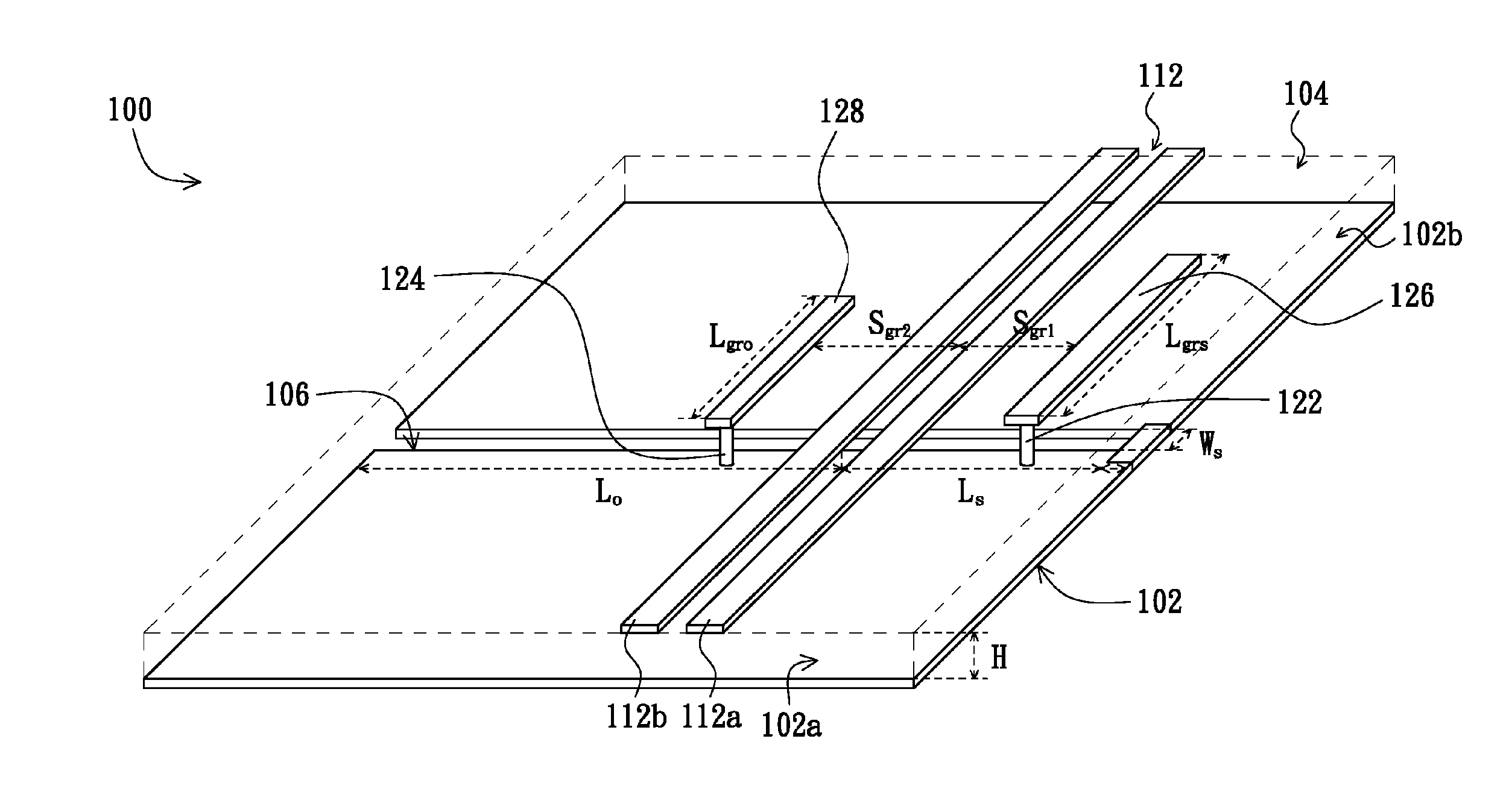
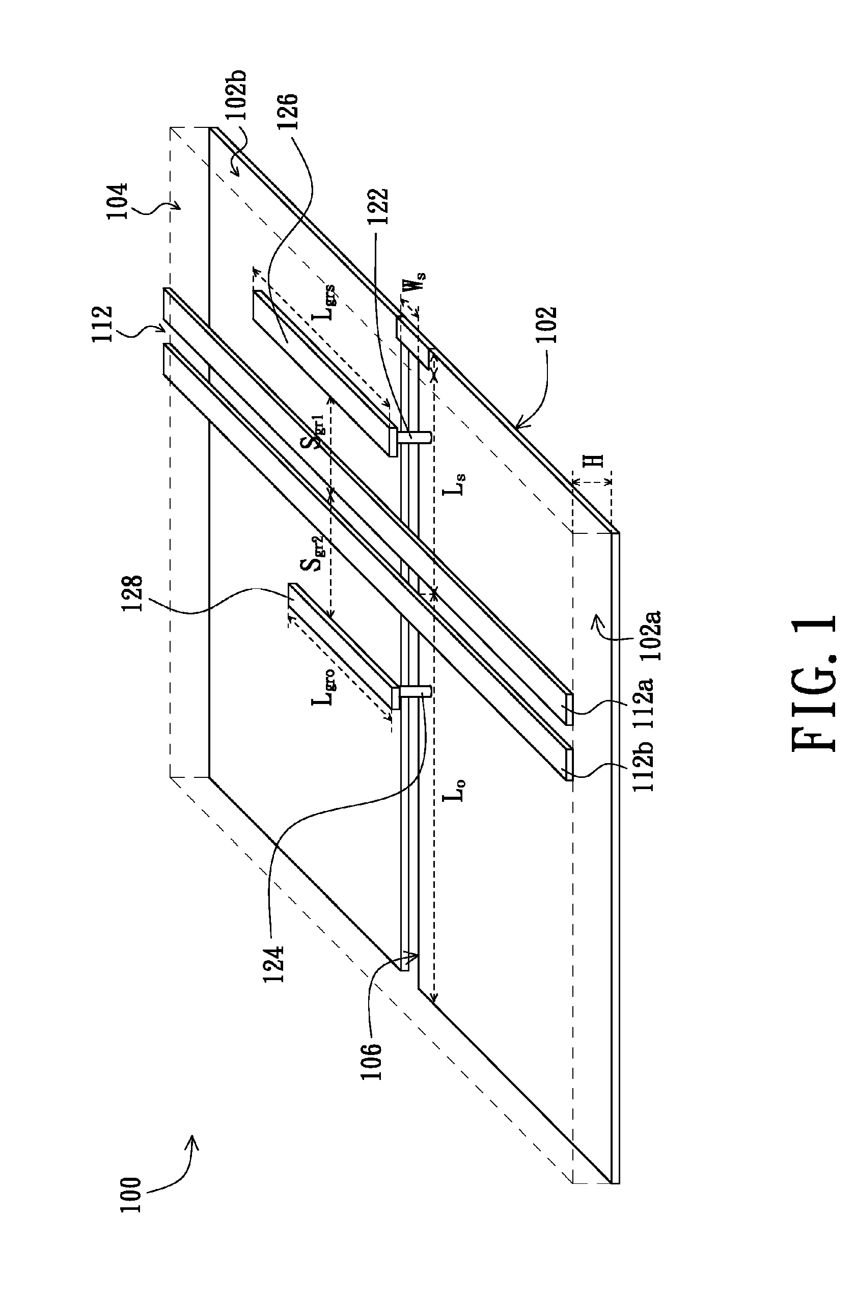
[0024]FIG. 1 is a structure view of an electric object in accordance with an exemplary embodiment of the present invention. Referring to FIG. 1, the electric object of the exemplary embodiment may be a circuit board 100, such as a printed circuit board, a flexible substrate or any of other circuit boards. In some other exemplary embodiments, the electric object 100 also may be an integrated circuit or any of other substrates. The electric object 100 of the exemplary embodiment has a plurality of electric surfaces, such as 102 and 104. These electric surfaces are opposite with each other, and each of the electric surfaces is space...


PUM

PropertyMeasurementUnit
thicknessaaaaaaaaaa
electricaaaaaaaaaa
structureaaaaaaaaaa

Abstract

A method for reducing EM radiation comprises at least one first resonance line disposed on one of electric surfaces, which is disposed at a side of a transmission line structure on one of the electric surface. The resonance line crosses over a slot of another electric surface. The slot is etched on a corresponding electric surface. In addition, the transmission line structure crosses over the slot of the electric surface. Then, the first resonance line connects the electric surface having the slot with another electric surface. It can adjust at least one of a length, a width and a shape of the first resonance line, to make an input impedance seen from a crossed point between the transmission line structure and the slot approximately 0.

Description

FIELD OF THE INVENTION[0001]The present invention relates to a technology for reducing EM (electromagnetic) radiation, and more particularly to a technology for reducing EM radiation generated by a structure of signal lines crossing over slots.BACKGROUND OF THE INVENTION[0002]With the rapid development of the science and technology, when active circuits operate in high-speed and operating frequencies thereof are increased, the active circuits require prompt supply of transient currents from the power distribution network (PDN) of package or printed circuit boards (PCBs). Then, simultaneous switching noises are generated to influence the normal operation of chips, and it is a problem which should be urgently solved. The conventional technology completely isolates the PCBs or a packaged structure by etching the slots between the power or ground layers, and it has been proved that it is very effectual to restrain the noise whose frequency is lower than GHz. Furthermore, it may design s...

Claims


Application Information

Patent Timeline
Patent Type & Authority Patents(United States)
IPC IPC(8): H04B3/28
CPCH05K1/0227H05K1/0239H01P3/026H05K1/0245H05K2201/09781Y10T29/49124H05K1/025
Inventor WU, TZONG-LINCHUANG, HAO-HSIANG
Owner NAT TAIWAN UNIV
Why Eureka
Try Eureka