
Organic light emitting diode display and driving method

a light-emitting diode and light-emitting diode technology, applied in the field of organic light-emitting diode displays, can solve the problems of low luminous efficiency and luminance of LEDs, narrow viewing angles, and high power consumption of LEDs, and achieve the effect of preventing color distortion

Active Publication Date: 2013-10-01
LG DISPLAY CO LTD
View PDF19 Cites 9 Cited by
  • Summary
  • Abstract
  • Description
  • Claims
  • Application Information

AI Technical Summary

Benefits of technology

This solution effectively maintains consistent luminance across different image display patterns and outdoor conditions, preventing color distortion by ensuring that driving currents for R, G, and B pixels are adjusted to achieve desired luminance levels, thereby stabilizing color representation.

Problems solved by technology

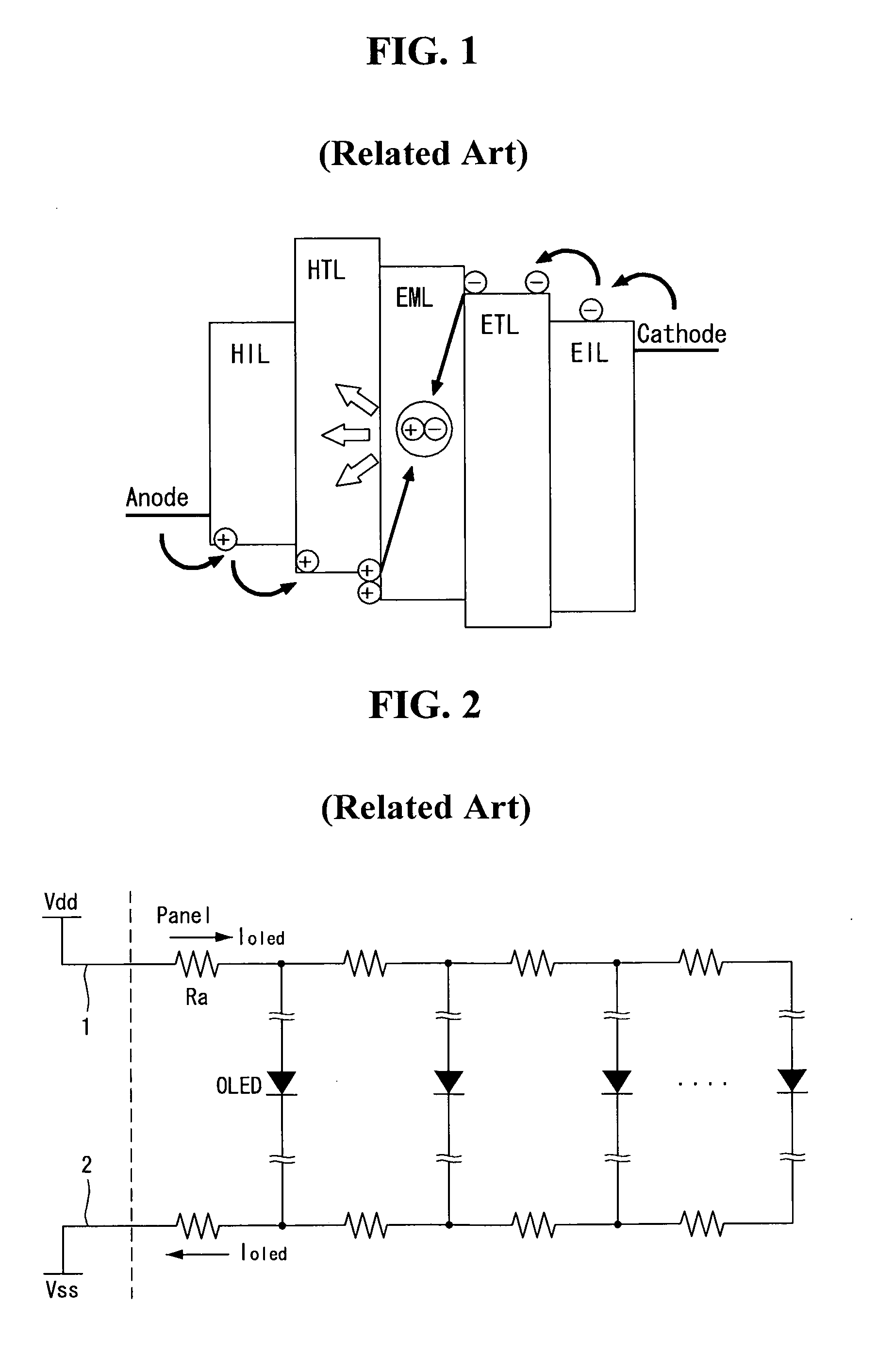
The PDP among them is simple in its structure and fabrication process, thus the PDP is light, thin, short and small and has been paid attention to as a display which is most advantageous in being made large-sized, but there is a big disadvantage in that the luminous efficiency and luminance thereof are low and the power consumption thereof is high.
A TFT LCD to which a thin film transistor (hereinafter, referred to as “TFT”) is applied as a switching device is one of the most widely used flat panel display, but has the problems of narrow viewing angle and low response speed because the TFT LCD is a non-light-emitting device.
However, such an organic light emitting diode display has the problems that the luminance is different for each of R, G, and B pixels (PB) depending on an image display pattern or an outdoor environmental condition, and this leads to color distortion.
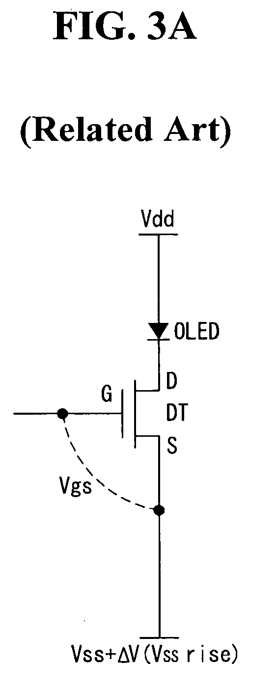
A more significant issue is that when the voltage Vgs between the gate and source of the driving TFT is changed depending on the image display pattern due to the IR drop, color coordinates are distorted.
As a result, as shown in FIG. 6, change in luminance according to a light emitting area is varied for each of the R, G, and B pixels, and hence color coordinates are distorted, thus causing color distortion.

Method used


Image

  • Organic light emitting diode display and driving method
  • Organic light emitting diode display and driving method
  • Organic light emitting diode display and driving method

Examples


Embodiment Construction

[0045]Hereinafter, an implementation of this document will be described in detail with reference to FIGS. 7 to 12.

[0046]FIG. 7 is a block diagram showing an organic light emitting diode display according to an exemplary embodiment of the present invention.

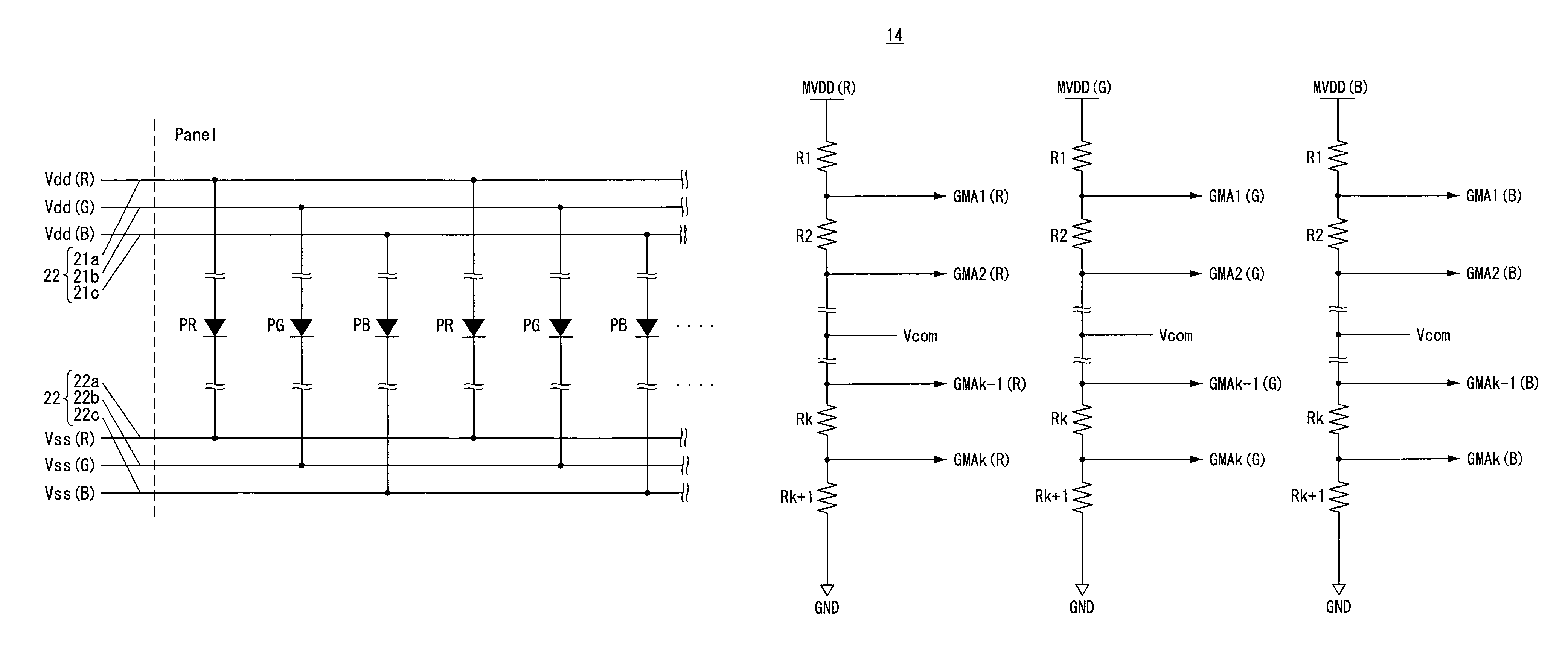
[0047]Referring to FIG. 7, the organic light emitting diode display according to the exemplary embodiment of the present invention includes a display panel 10, a timing controller 11, a current estimating circuit 11a, a current sensing circuit 12, a gamma power source control circuit 13, a gamma reference voltage generating circuit 14, a data driving circuit 15, a gate driving circuit 16, and a driving voltage supply circuit 17.

[0048]The display panel 10 has a plurality of data lines DL and a plurality of gate lines GL that are crossed to each other. Cross points of the plurality of data lines DL and the plurality of gate lines GL define R, G, and B pixels PR, PG, and PB that are disposed in matrix. The R pixel PR includes an R org...


PUM


Abstract

An OLED display including a display panel having a plurality of R, G, and B pixels formed and at least one of a high-potential and low-potential driving voltage supply line disposed; a data driving circuit; a gamma reference voltage generating circuit for generating gamma reference voltages for R, G, and B by dividing voltages of high-potential gamma power sources; a current estimating circuit for generating digital estimated current values for R, G, and B; a current sensing circuit for generating digital sensing current values for R, G, and B; and a gamma power source control circuit for controlling the high-potential gamma power sources by comparing the digital estimated current values for R, G, and B with the digital sensing current values for R, G, and B so that driving currents corresponding to the respective digital estimated current values flow in the respective R, G, and B pixels.

Description

[0001]This application claims the benefit of Korean Patent Application No. 10-2009-0037645 filed on Apr. 29, 2009, which is incorporated herein by reference for all purposes as if fully set forth herein.BACKGROUND OF THE INVENTION[0002]1. Field of the Invention[0003]This document relates to an organic light emitting diode display, and more particularly, to an organic light emitting diode display, which can prevent luminance change and color distortion that are caused by an image display pattern or an outdoor environmental condition.[0004]2. Discussion of the Related Art[0005]Recently, there has been developed various flat panel display that can reduce their weight and size which were disadvantages of a cathode ray tube. The flat panel display includes a liquid crystal display (hereinafter, referred to as “LCD”), a field emission display FED, a plasma display panel (hereinafter, referred to as “PDP”), an electroluminescence EL, and the like.[0006]The PDP among them is simple in its s...

Claims


Application Information

Patent Timeline
Patent Type & Authority Patents(United States)
IPC IPC(8): G09G3/30
CPCG09G3/3233G09G3/3291G09G2310/027G09G2320/0223G09G2320/029G09G2320/041G09G2320/043G09G2320/0673G09G2330/021G09G3/20G09G3/30
Inventor BYUN, SEUNGCHAN
Owner LG DISPLAY CO LTD
Learn More