Remote plasma burn-in

a plasma burnin and plasma technology, applied in the direction of chemical vapor deposition coating, coating, electric discharge tube, etc., can solve the problems of dielectric material, dielectric material, and the structural features of the device having decreased spatial dimensions,

Inactive Publication Date: 2013-10-08
APPLIED MATERIALS INC
View PDF445 Cites 162 Cited by
  • Summary
  • Abstract
  • Description
  • Claims
  • Application Information

AI Technical Summary

Problems solved by technology

The decreasing feature sizes result in structural features on the device having decreased spatial dimensions.
The widths of gaps and trenches on the device narrow to a point where the aspect ratio of gap depth to its width becomes high enough to make it challenging to fill the gap with dielectric material.
The depositing dielectric material is prone to clog at the top before the gap completely fills, producing a void or seam in the middle of the gap.
However, once these highly flowable materials are deposited, they have to be hardened into a solid dielectric material.

Method used


Image

  • Remote plasma burn-in
  • Remote plasma burn-in
  • Remote plasma burn-in

Examples


Embodiment Construction

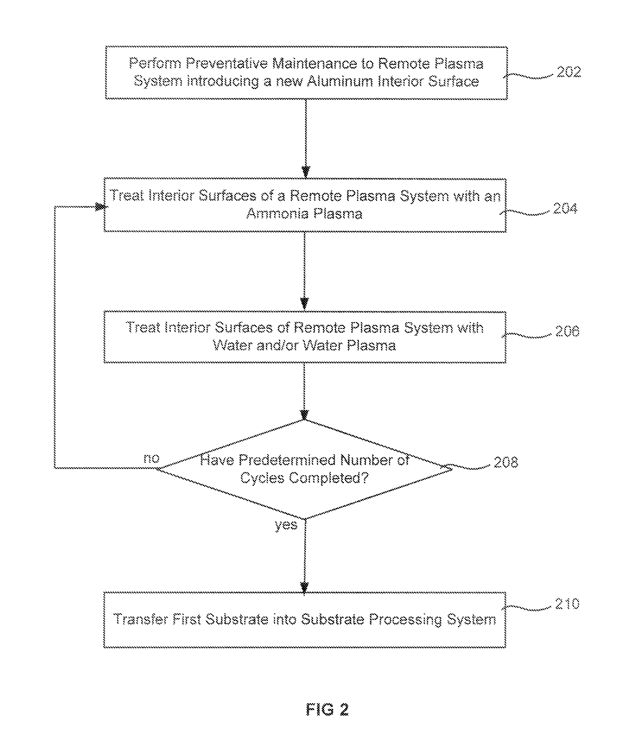
[0015]Methods of treating the interior of a plasma region are described. The methods include a preventative maintenance procedure or the start-up of a new substrate processing chamber having a remote plasma system. A new interior surface is exposed within the remote plasma system. The (new) interior surfaces are then treated by sequential steps of (1) forming a remote plasma from hydrogen-containing precursor within the remote plasma system and then (2) exposing the interior surfaces to water vapor. Steps (1)-(2) are repeated at least ten times to complete the burn-in process. Following the treatment of the interior surfaces, a substrate may be transferred into a substrate processing chamber. A dielectric film may then be formed on the substrate by flowing one precursor through the remote plasma source and combining the plasma effluents with a second precursor flowing directly to the substrate processing region.

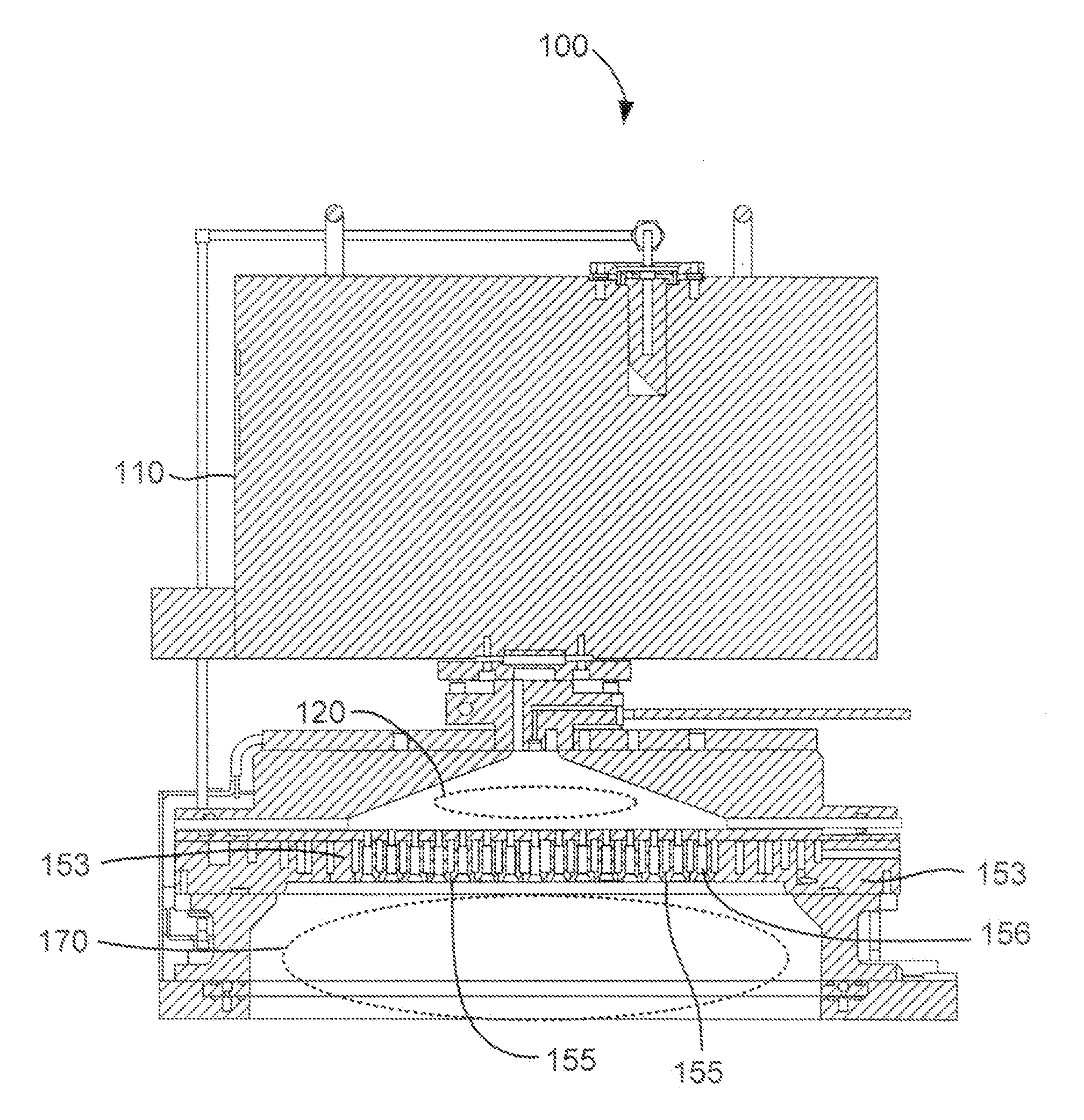
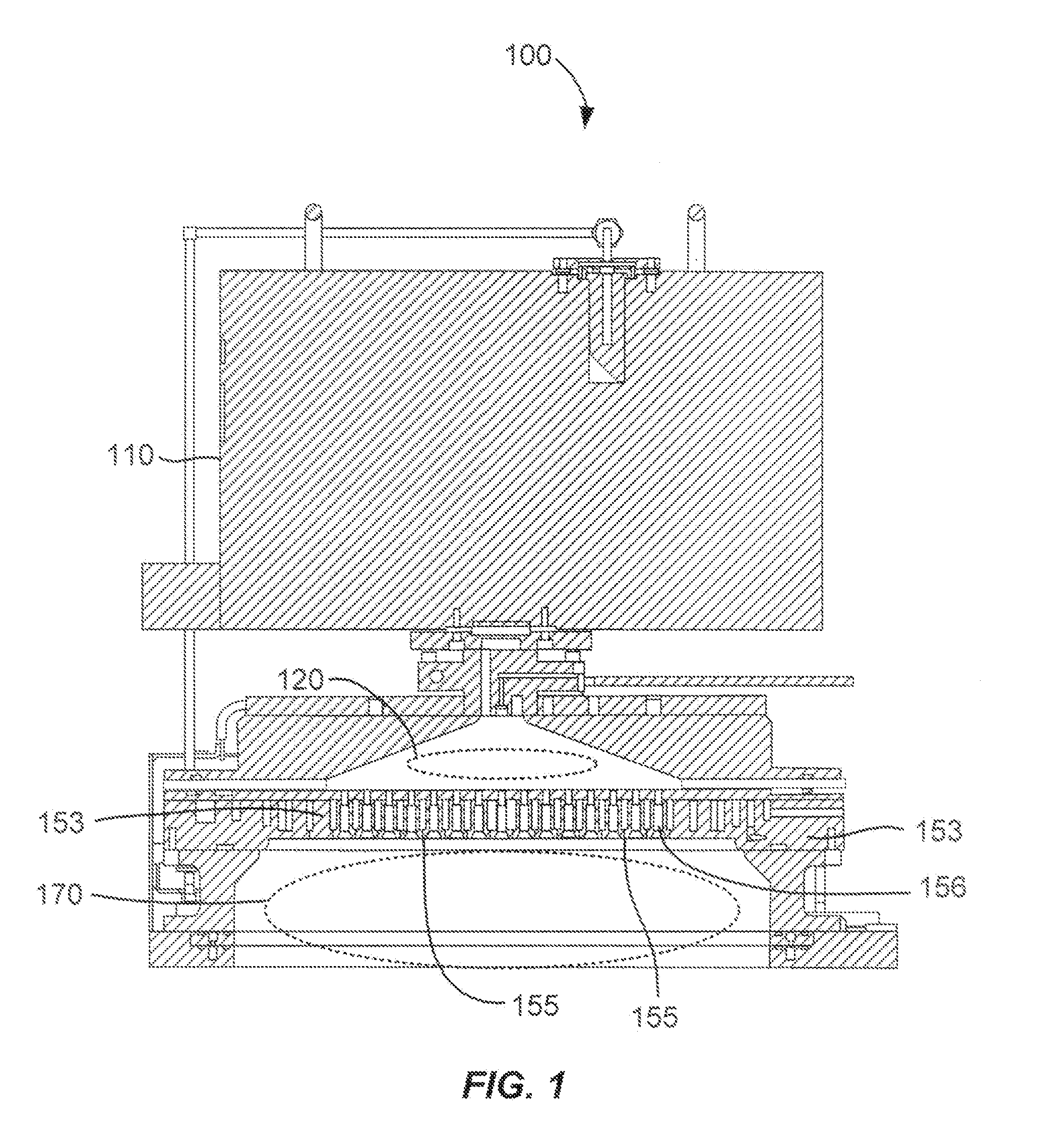
[0016]A brief description of an exemplary substrate processing chamber l...


PUM

PropertyMeasurementUnit
plasma poweraaaaaaaaaa
pressureaaaaaaaaaa

Abstract

Methods of treating the interior of a plasma region are described. The methods include a preventative maintenance procedure or the start-up of a new substrate processing chamber having a remote plasma system. A new interior surface is exposed within the remote plasma system. The (new) interior surfaces are then treated by sequential steps of (1) forming a remote plasma from hydrogen-containing precursor within the remote plasma system and then (2) exposing the interior surfaces to water vapor. Steps (1)-(2) are repeated at least ten times to complete the burn-in process. Following the treatment of the interior surfaces, a substrate may be transferred into a substrate processing chamber. A dielectric film may then be formed on the substrate by flowing one precursor through the remote plasma source and combining the plasma effluents with a second precursor flowing directly to the substrate processing region.

Description

CROSS-REFERENCES TO RELATED APPLICATIONS[0001]This application claims the benefit of U.S. Prov. Pat. App. No. 61 / 543,159 filed Oct. 4, 2011, and entitled “REMOTE PLASMA BURN-IN,” which is entirely incorporated herein by reference for all purposes.BACKGROUND OF THE INVENTION[0002]Semiconductor device geometries have dramatically decreased in size since their introduction several decades ago. Modern semiconductor fabrication equipment routinely produces devices with 32 nm, 28 nm and 22 nm feature sizes, and new equipment is being developed and implemented to make devices with even smaller geometries. The decreasing feature sizes result in structural features on the device having decreased spatial dimensions. The widths of gaps and trenches on the device narrow to a point where the aspect ratio of gap depth to its width becomes high enough to make it challenging to fill the gap with dielectric material. The depositing dielectric material is prone to clog at the top before the gap compl...

Claims


Application Information

Patent Timeline
Patent Type & Authority Patents(United States)
IPC IPC(8): H01L21/31
CPCC23C16/345C23C16/452C23C16/56H01L21/02164H01L21/02211H01L21/02219H01L21/02274H01L21/02326H01J37/32357H01J37/32862
Inventor LIANG, JINGMEIJI, LILIINGLE, NITIN K.
Owner APPLIED MATERIALS INC
Why Eureka
Try Eureka