Stretchable and foldable electronic devices

a technology of electronic devices and foldable parts, applied in the direction of dielectric characteristics, circuit bendability/stretchability, coatings, etc., can solve the problems inability to withstand the force of mechanical force, etc., to achieve the effect of facilitating design and manufacture, reducing or eliminating the influence of mechanical strain on the performance of electronic devices

Active Publication Date: 2013-10-08
THE BOARD OF TRUSTEES OF THE UNIV OF ILLINOIS
View PDF213 Cites 225 Cited by
  • Summary
  • Abstract
  • Description
  • Claims
  • Application Information

AI Technical Summary

Benefits of technology

[0012]Highly bendable and stretchable electronic devices, and methods for making such devices, are accessed by controlling the location of a neutral mechanical surface to correspond to strain-sensitive layers or by selective use of strain isolation layers to isolate strain-sensitive layers from applied stresses and strains. The processes and devices are useful in a wide range of applications and devices such as electronic and optoelectronic systems in curved systems and systems that undergo mechanical deformation. The processes and devices combine high quality electronic materials, such as aligned arrays of silicon nanoribbons and other inorganic nanomaterials, with ultrathin and elastomeric substrates, in multilayer neutral mechanical plane designs and with an optionally ‘wavy’ structural layout. Such approaches, guided by detailed mechanics models, facilitate design and manufacture of diverse classes of integrated circuits as well as highly integrated optoelectronics systems with well-developed electronic materials, whose intrinsic brittle, fragile mechanical properties would otherwise preclude their use in such applications The systems and processes are capable of providing strain-independent electrical devices at a performance level comparable to state-of-the-art devices built on brittle semiconductor wafers. For example, systems provided herein minimize or eliminate the influence of mechanical strain on device performance, thereby facilitating the use of such devices in a wide range of applications and of any arbitrary geometry. In other aspects, the systems provided herein access shape-conforming electronic devices that would otherwise undergo strain-induced mechanical failure.
[0013]Processes provided herein are optionally compatible with conventional electronics manufacturing processes that are intrinsically planar in nature due to the patterning, deposition, etching, materials growth and doping methods used in those existing fabrication processes. Stretchable and compressible systems provided herein avoid planar geometry limitations by facilitating a geometric transformation of conventional planar geometry manufacturing systems to an arbitrarily curvilinear shape for use in applications requiring non-linear geometry. Accordingly, processes provided herein permit integration of planar device technologies onto surfaces of complex curvilinear objects.

Problems solved by technology

The design and fabrication of flexible electronic devices exhibiting good electronic performance, however, present a number of significant challenges.
First, the well developed methods of making conventional silicon based electronic devices are incompatible with most flexible materials.
In addition, most inorganic semiconductors are not intrinsically soluble in convenient solvents that would allow for solution based processing and delivery.
Second, although many amorphous silicon, organic or hybrid organic-inorganic semiconductors are compatible with incorporation into flexible substrates and can be processed at relatively low temperatures, these materials do not have electronic properties capable of providing integrated electronic devices capable of good electronic performance.
As a result of these limitations, flexible electronic devices are presently limited to specific applications not requiring high performance, such as use in switching elements for active matrix flat panel displays with non-emissive pixels and in light emitting diodes.
These circuits often are unable to sufficiently conform to their surroundings because of an inability of the conducting components to stretch in response to conformation changes.
Accordingly, those flexible circuits are prone to damage, electronic degradation and can be unreliable under rigorous and / or repeated conformation change.
The drawbacks of a conductive rubber include high electrical resistivity and significant resistance changes under stretching, thereby resulting in overall poor interconnect performance and reliability.
That system suffers limitations in the ability to controllably and precisely pattern in different shapes and in additional planes, thereby limiting the ability to tailor systems to different strain and bending regimes.
Those metal cracks, however, are not compatible with thick metal films, and instead is compatible with a rather narrow range of thin metal films (e.g., on the order of less than 30 nm) that are deposited on top of patterned elastomer.
That study, however, used comparatively thin layers of metal films (e.g., about 105 nm) and is relatively limited in that the system could potentially make electrical conductors that could be stretched by about 10%.

Method used


Image

  • Stretchable and foldable electronic devices
  • Stretchable and foldable electronic devices
  • Stretchable and foldable electronic devices

Examples


example 1

Stretchable and Foldable Silicon Integrated Circuits

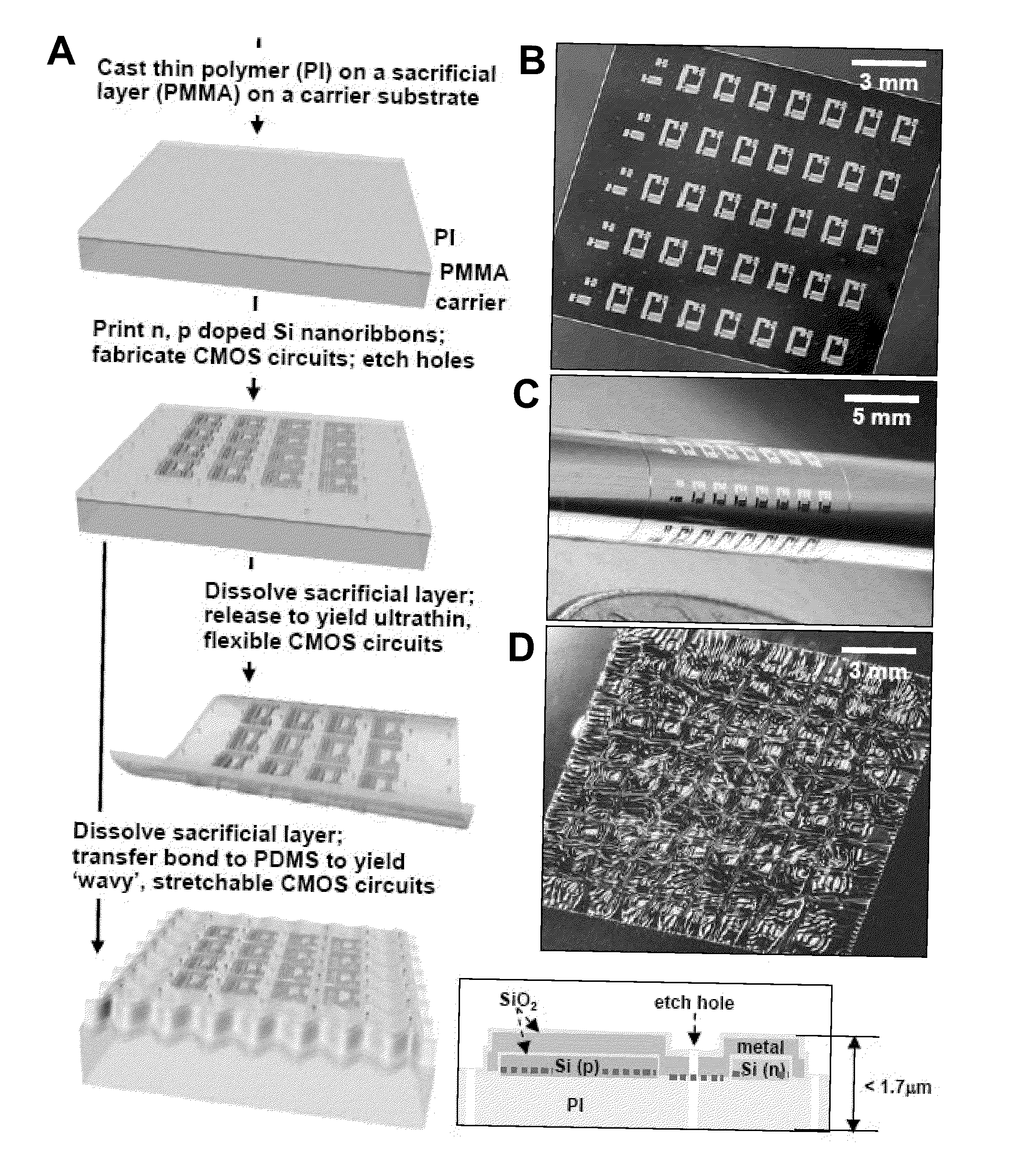
[0165]Disclosed herein are approaches to access high performance, stretchable and foldable integrated circuits (ICs). The systems integrate inorganic electronic materials, including aligned arrays of nanoribbons of single crystalline silicon, with ultrathin plastic and elastomeric substrates. The designs combine multilayer neutral mechanical plane layouts and ‘wavy’ structural configurations in silicon complementary logic gates, ring oscillators and differential amplifiers. Three dimensional analytical and computational modeling of the mechanics of deformations in these ICs, together with circuit simulations, illuminate aspects that underlie the measured behaviors. The strategies represent general and scalable routes to high performance, foldable and stretchable optoelectronic devices that can incorporate established, high performance inorganic electronic materials whose fragile, brittle mechanical properties would otherwise preclu...

example 2

A Hemispherical Electronic Eve Camera Based on Compressible Silicon Optoelectronics

[0218]The human eye represents a remarkable imaging device, with many attractive design features.1,2 Prominent among these is a hemispherical detector geometry, similar to that found in many other biological systems, that enables wide field of view and low aberrations with simple, few component, imaging optics. This type of configuration is extremely difficult to achieve using established optoelectronics technologies, due to the intrinsically planar nature of the patterning, deposition, etching, materials growth and doping methods that exist for fabricating such systems. This example provides processes and related systems that avoid these apparent limitations. The devices and processes are used to yield high performance, hemispherical electronic eye cameras based on single crystalline silicon technology. The approach uses wafer-scale optoelectronics formed in unusual, two dimensionally compressible co...

example 3

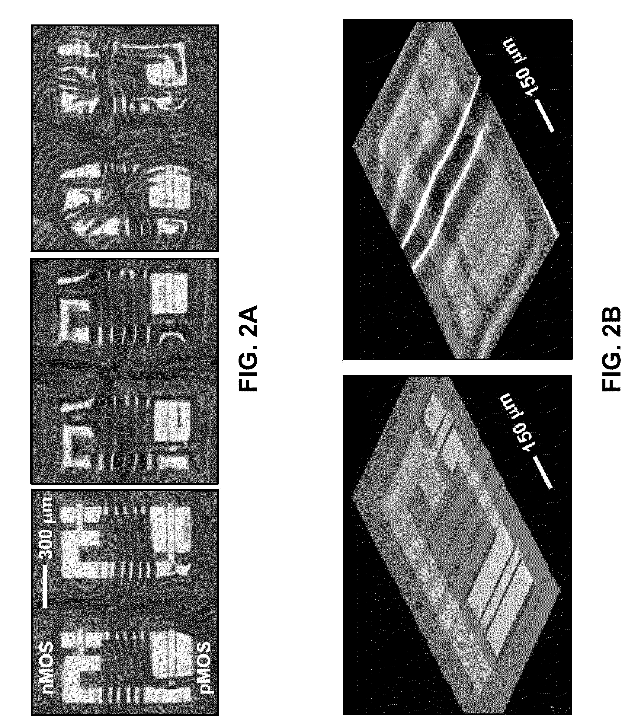
CMOS Integrated Circuits with Monolithically Integrated Stretchable Wavy Interconnects

[0302]Stretchable CMOS circuits comprising ultrathin active devices mechanically and electrically connected by narrow metal lines and polymer bridging structures are presented. This layout, together with designs that locate the neutral mechanical plane near the critical circuit layers yields strain independent electrical performance and realistic paths to circuit integration. Mechanical and electrical modeling and experimental characterization reveal the underlying physics of these systems.

[0303]Stretchable electronics is emerging as a technology that could be valuable for various applications, such as conformal personal or structural health monitors and hemispherical detector arrays. Such devices cannot be accomplished with conventional wafer based circuits or even with more recent systems that offer simple mechanical bendability. Presently, two approaches exist for achieving stretchability via th...


PUM

PropertyMeasurementUnit
temperaturesaaaaaaaaaa
fracture strainsaaaaaaaaaa
distanceaaaaaaaaaa

Abstract

Disclosed herein are stretchable, foldable and optionally printable, processes for making devices and devices such as semiconductors, electronic circuits and components thereof that are capable of providing good performance when stretched, compressed, flexed or otherwise deformed. Strain isolation layers provide good strain isolation to functional device layers. Multilayer devices are constructed to position a neutral mechanical surface coincident or proximate to a functional layer having a material that is susceptible to strain-induced failure. Neutral mechanical surfaces are positioned by one or more layers having a property that is spatially inhomogeneous, such as by patterning any of the layers of the multilayer device.

Description

CROSS-REFERENCE TO RELATED APPLICATIONS[0001]This application claims benefit of U.S. Provisional Patent App. Nos. 61 / 033,886, filed Mar. 5, 2008, 61 / 061,978 filed Jun. 16, 2008, and 61 / 084,045 filed Jul. 28, 2008, each of which are specifically incorporated by reference herein to the extent not inconsistent with the present application.STATEMENT REGARDING FEDERALLY SPONSORED RESEARCH OR DEVELOPMENT[0002]This invention was made at least in part with U.S. government support under DMI-0328162 and ECCS-0824129 awarded by the National Science Foundation and under DEFG02-91 ER45439, DEFG02-07ER46471 and DEFG02-07ER46453 awarded by the Department of Energy. The U.S. government has certain rights in the invention.BACKGROUND OF INVENTION[0003]Since the first demonstration of a printed, all polymer transistor in 1994, a great deal of interest has been directed at a potential new class of electronic systems comprising flexible integrated electronic devices on plastic substrates. [Garnier, F., ...

Claims


Application Information

Patent Timeline
Patent Type & Authority Patents(United States)
IPC IPC(8): H05K1/00
CPCH01L21/4867H01L23/4985H01L25/50H05K1/0283H05K3/207H05K1/03H01L21/6835Y10T29/49002H01L25/0655H01L27/14601H01L2221/68359H01L2224/05624H01L2924/01046H01L2924/01057H01L2924/01079H01L2924/09701H01L2924/12044H01L2924/3025H05K1/036H05K1/0393H05K1/16H05K2201/0133H05K2203/0271H01L2924/01019H01L2924/13091H01L2924/1461H01L2924/00Y10T29/4913Y10T29/49146B33Y80/00H01L27/1218H05K1/185H05K3/284H05K3/30H05K1/028H05K1/111H05K1/118
Inventor ROGERS, JOHN A.HUANG, YONGGANGKO, HEUNG CHOSTOYKOVICH, MARKCHOI, WON MOOKSONG, JIZHOUAHN, JONG HYUNKIM, DAE HYEONG
Owner THE BOARD OF TRUSTEES OF THE UNIV OF ILLINOIS
Why Eureka
Try Eureka