Integrated decoupling capacitor employing conductive through-substrate vias

a decoupling capacitor and through-substrate technology, applied in capacitors, semiconductor devices, semiconductor/solid-state device details, etc., can solve the problems of adverse effects on the performance of off-chip drivers, the increase of reference supplies, and the performance of internal devices. achieve the effect of reducing high frequency noise and low inductan

Active Publication Date: 2013-10-15
TESSERA INC
View PDF71 Cites 17 Cited by
  • Summary
  • Abstract
  • Description
  • Claims
  • Application Information

AI Technical Summary

Benefits of technology

[0007]According to an embodiment of the present invention, a capacitor in a semiconductor substrate employs a conductive through-substrate via (TSV) as an inner electrode and a columnar doped semiconductor region as an outer electrode. The capacitor provides a large decoupling capacitance in a small area, and does not impact circuit density or a Si3D structural design. Additional conductive TSV's can be provided in the semiconductor substrate to provide electrical connection for power supplies and signal transmission therethrough. The capacitor has a lower inductance than a conventional array of capacitors having comparable capacitance, thereby enabling reduction of high frequency noise in the power supply system of stacked semiconductor chips.

Problems solved by technology

This results in an increase in the noise generated on the reference supplies.
As this noise increases, the performance of the internal devices as well as the performance of off-chip drivers is adversely impacted due to the reduction of noise margins available for the system design.

Method used


Image

  • Integrated decoupling capacitor employing conductive through-substrate vias
  • Integrated decoupling capacitor employing conductive through-substrate vias
  • Integrated decoupling capacitor employing conductive through-substrate vias

Examples


first embodiment

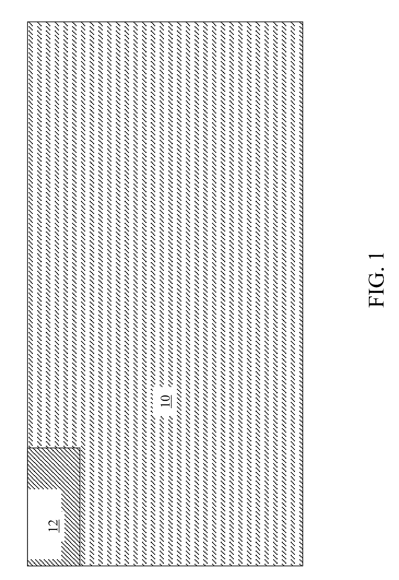
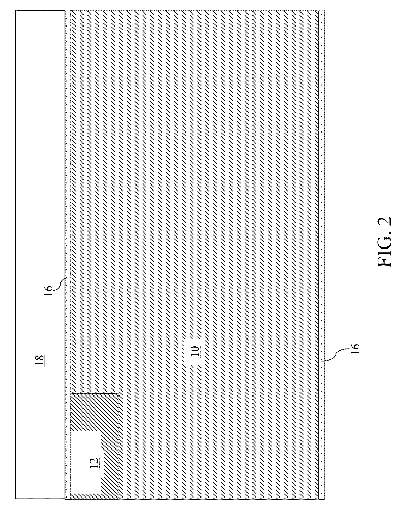
[0024]Referring to FIG. 1, a first exemplary structure according to the present invention includes a semiconductor substrate 10 that has a semiconductor material. The semiconductor material of the semiconductor substrate 10 can be selected from, but is not limited to, silicon, germanium, silicon-germanium alloy, silicon carbon alloy, silicon-germanium-carbon alloy, gallium arsenide, indium arsenide, indium phosphide, III-V compound semiconductor materials, II-VI compound semiconductor materials, organic semiconductor materials, and other compound semiconductor materials. Preferably, the semiconductor material of the semiconductor substrate 10 is a single crystalline material. For example, the semiconductor substrate 10 can be a single crystalline silicon layer. The semiconductor substrate 10 can be doped with dopants of a first conductivity type, which can be p-type or n-type. The dopant concentration of the semiconductor substrate 10 can be from 1.0×10¹⁴ / cm3 to 1.0×10¹⁷ / cm3.

[0025]A...

second embodiment

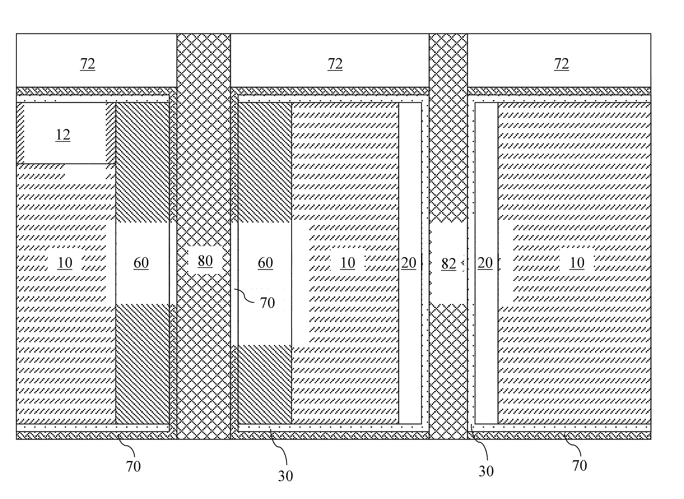
[0048]Referring to FIG. 19, a second exemplary structure according to the present invention includes a packaging substrate 200, a plurality of first semiconductor chips 100, a plurality of second semiconductor chips 300, an array of first solder balls 199 electrically connecting each of the first semiconductor chips 100 to the packaging substrate 200, and an array of second solder balls 299 electrically connecting each of the second semiconductor chips 300 to a first semiconductor chip 100. Each of the first semiconductor chips 100 includes at least one capacitor 180 and at least one laterally-insulated conductive through-substrate connection structure 182. The first semiconductor chips 100 may, or may not, include additional semiconductor devices such as field effect transistors, bipolar transistors, thyristors, and diodes. The second semiconductor chips 300 can include any type of semiconductor devices.

[0049]The capacitors 180 can function as decoupling capacitors that reduce nois...

third embodiment

[0050]Referring to FIG. 20, a third exemplary structure according to the present invention includes a packaging substrate 200, a interposer structure 400, a plurality of first semiconductor chips 100, and a plurality of second semiconductor chips 300. An array of first solder balls 199 electrically connects each of the first semiconductor chips 100 to the interposer structure 400. An array of second solder balls 299 electrically connects each of the second semiconductor chips 300 to a first semiconductor chip 100. An array of third solder balls 399 connects the interposer structure 400 to the packaging substrate 200.

[0051]The interposer structure 400 can include an interposer structure substrate layer 410, a lower dielectric material layer 420, and an upper dielectric material layer 430. The interposer structure substrate layer 410 includes a plurality of through-substrate via structures that are schematically illustrated as vertical lines. The plurality of through-substrate via str...


PUM


Abstract

A capacitor in a semiconductor substrate employs a conductive through-substrate via (TSV) as an inner electrode and a columnar doped semiconductor region as an outer electrode. The capacitor provides a large decoupling capacitance in a small area, and does not impact circuit density or a Si3D structural design. Additional conductive TSV's can be provided in the semiconductor substrate to provide electrical connection for power supplies and signal transmission therethrough. The capacitor has a lower inductance than a conventional array of capacitors having comparable capacitance, thereby enabling reduction of high frequency noise in the power supply system of stacked semiconductor chips.

Description

BACKGROUND[0001]The present invention relates to the field of semiconductor structures, and particularly to a decoupling capacitor that employs a conductive through-substrate via and methods of manufacturing the same.[0002]In resent years, “three dimensional silicon” (3DSi) structures have been proposed to enable joining of multiple silicon chips and / or wafers that are mounted on a package or a system board. The 3DSi structures increase the density of active circuits that are integrated in a given space.[0003]As the circuit density increases unit area, the amount of switching activity per unit area also increases. This results in an increase in the noise generated on the reference supplies. As this noise increases, the performance of the internal devices as well as the performance of off-chip drivers is adversely impacted due to the reduction of noise margins available for the system design.[0004]At present, this noise is controlled by embedding deep trench capacitors (DTC) within a...

Claims


Application Information

Patent Timeline
Patent Type & Authority Patents(United States)
IPC IPC(8): H01L27/108H01L21/02H01L23/04H01L29/94
CPCH01L21/76898H01L23/481H01L28/40H01L23/642H01L25/0657H01L2924/1305H01L2924/1301H01L2924/10253H01L2924/3011H01L23/49827H01L24/16H01L2224/13025H01L2225/06513H01L2225/06541H01L2924/01078H01L2924/12044H01L2924/15311H01L2924/19041H01L2924/30105H01L2924/30107H01L2924/00H01L21/8221H01L23/5222H01L27/0688
Inventor KIM, TAE HONGSPROGIS, EDMUND J.MCALLISTER, MICHAEL F.SHAPIRO, MICHAEL J.
Owner TESSERA INC
Why Eureka
Try Eureka