
Method for checking alignment accuracy of thin film transistor including performing a close/open circuit test

a thin film transistor and alignment accuracy technology, applied in the field of alignment accuracy testing of thin film transistors, can solve the problems of inability to improve sampling rate, adverse effects on desired circuits, and low metrologies, so as to achieve easy and fast testing results, increase sampling rate, and reduce the effect of measurement time for checking alignment accuracy of

Inactive Publication Date: 2013-11-12
CHUNGHWA PICTURE TUBES LTD
View PDF16 Cites 0 Cited by
  • Summary
  • Abstract
  • Description
  • Claims
  • Application Information

AI Technical Summary

Benefits of technology

[0010]According to the method for checking alignment accuracy of a TFT provided by the present invention, the first contact hole is formed simultaneously with forming the semiconductor structure, the source / drain, the pixel electrode, or the second contact hole for electrically connecting the pixel electrode and the source / drain of the TFT. When the first contact hole is not accurately aligned and formed, the connecting electrode, the first terminal and the second terminal of the testing device are not electrically connected to each other, and thus open circuit is obtained. Accordingly, alignment inaccuracy of the patterning process for forming the first contact hole and the corresponding layer is confirmed. Furthermore, the method for checking alignment accuracy of a TFT provided by the present invention is operated as a close / open circuit test, therefore the test results are easily and speedily obtained. Accordingly, measurement time for checking alignment accuracy of a TFT is substantially reduced and sampling rate is increased.

Problems solved by technology

In such cases, the desired circuit is adversely impacted, even is failed.
Accordingly, conventional optical metrologies suffer low sampling rates and such sampling rates cannot be improved due to the long measurement time.
In addition, the prior art even increases the amount of the measurement systems for increasing the sampling rates.
However, it still suffers high process cost.

Method used


Image

  • Method for checking alignment accuracy of thin film transistor including performing a close/open circuit test
  • Method for checking alignment accuracy of thin film transistor including performing a close/open circuit test
  • Method for checking alignment accuracy of thin film transistor including performing a close/open circuit test

Examples


Embodiment Construction

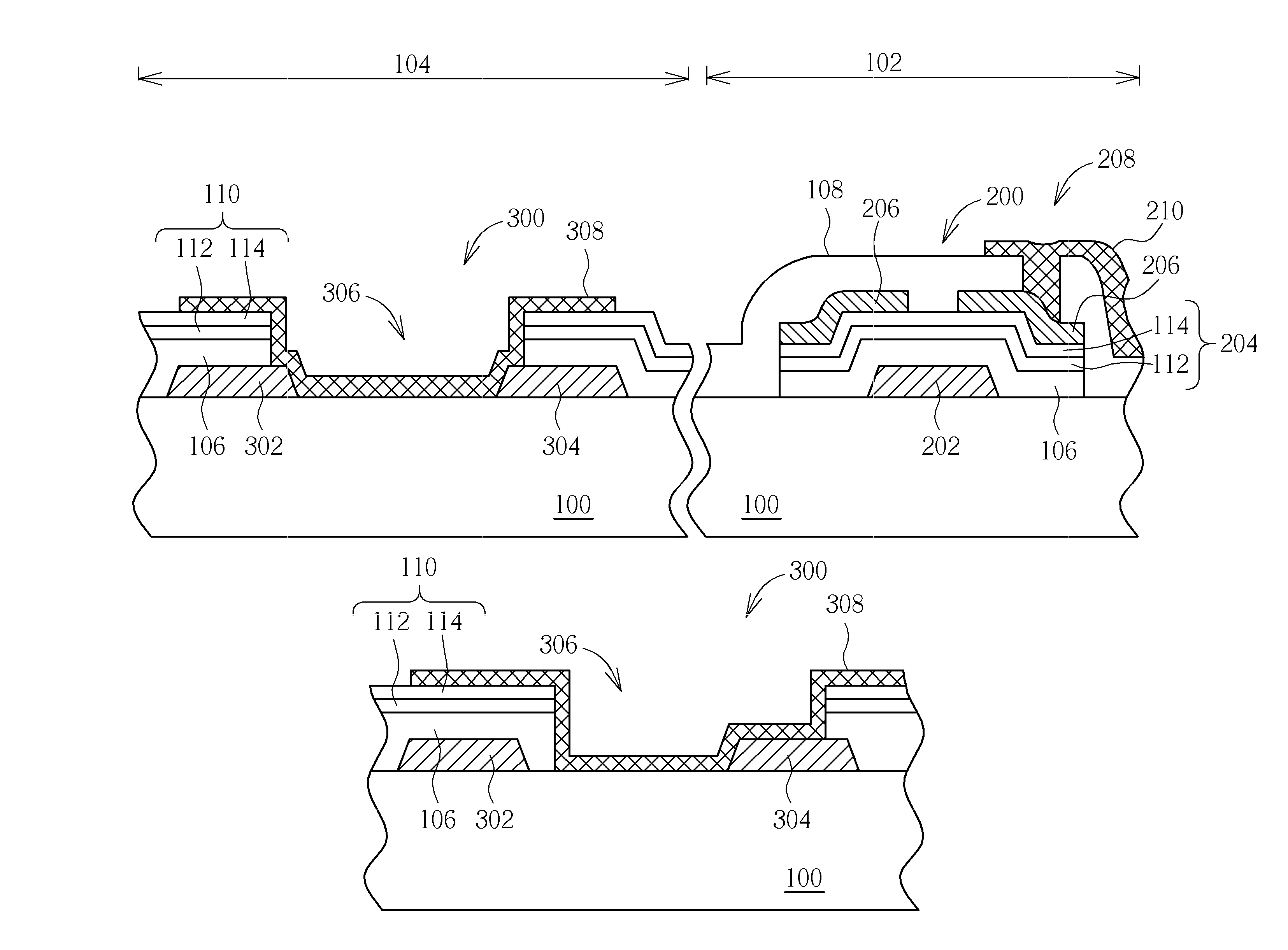
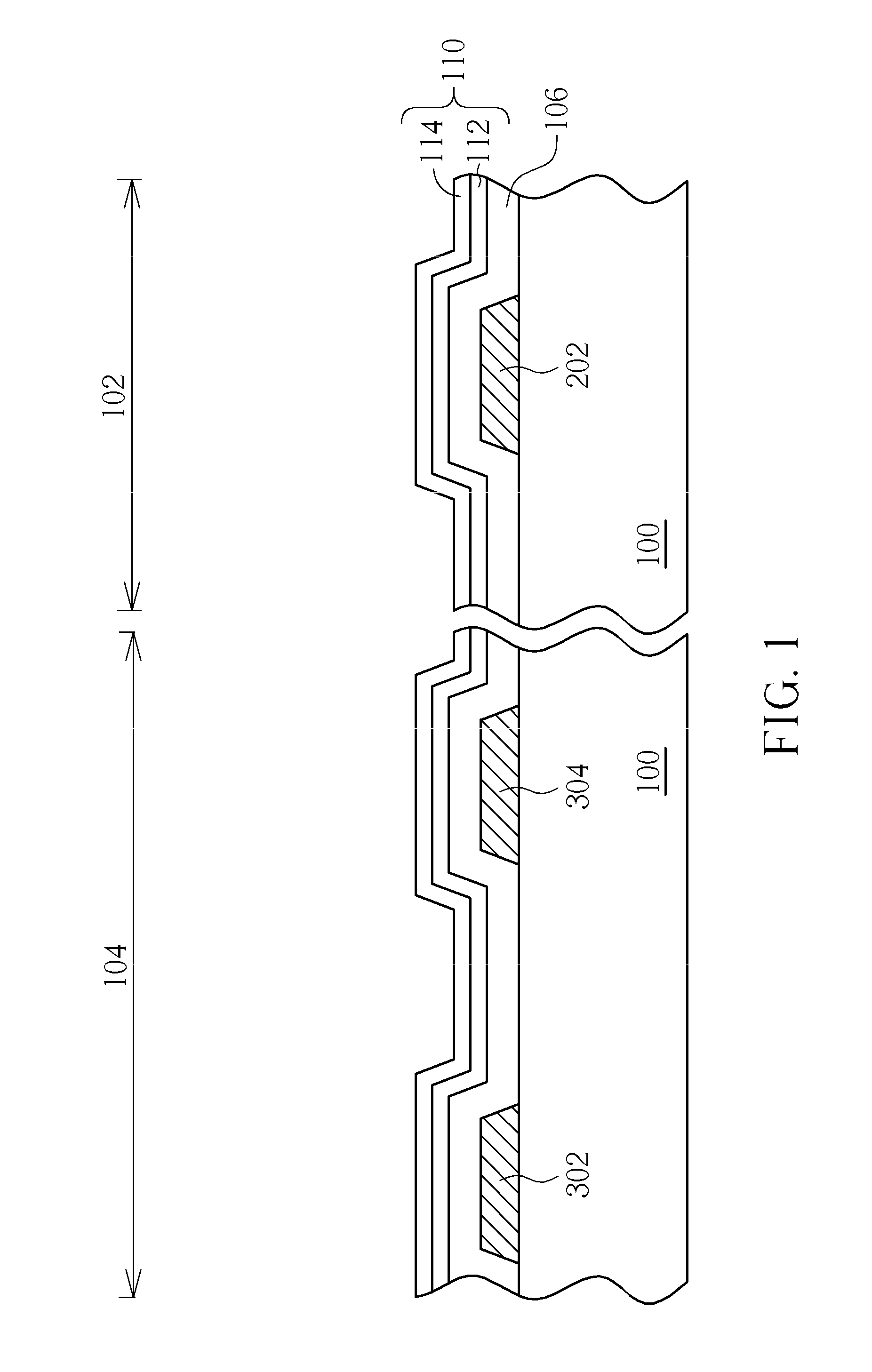
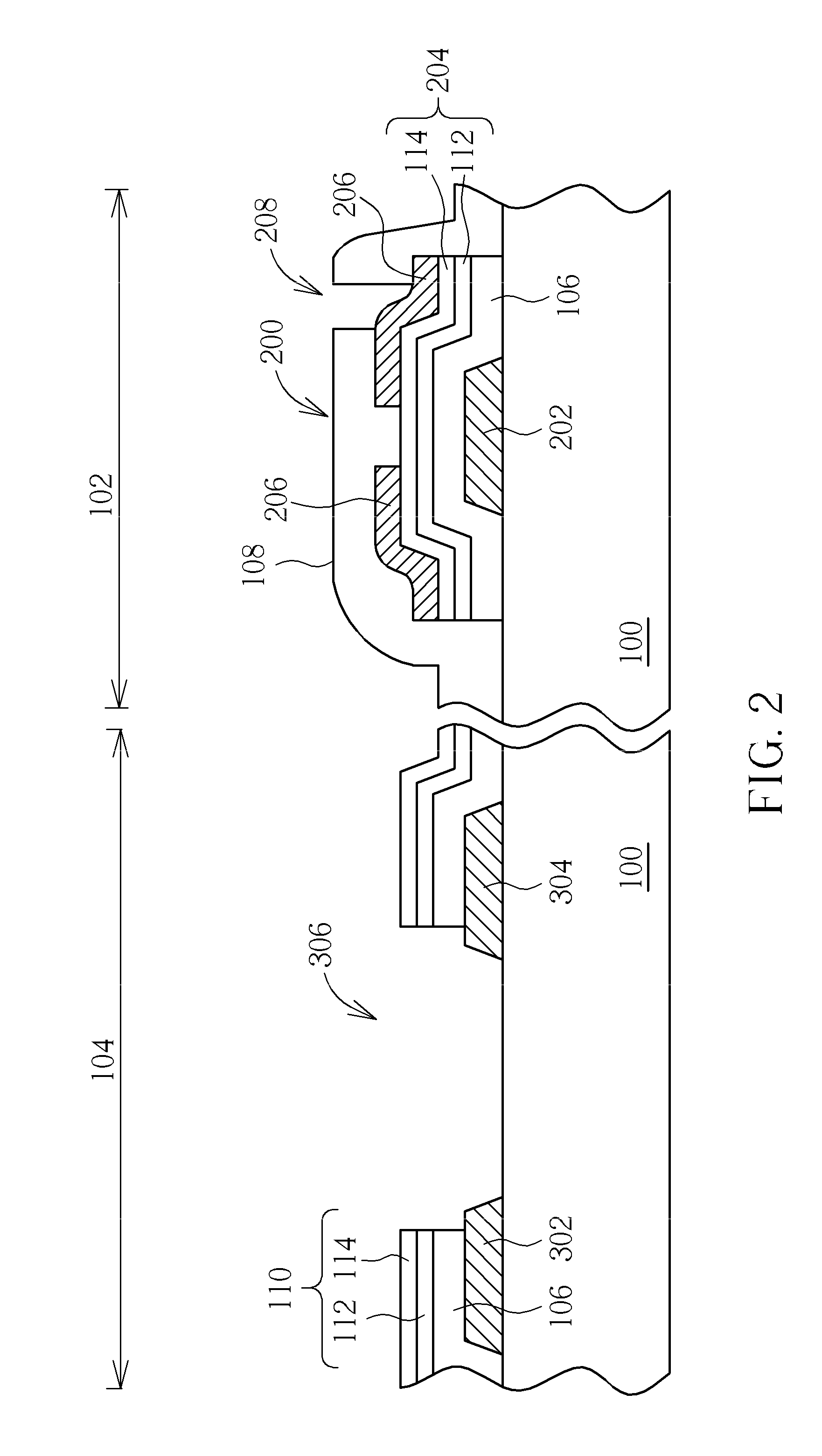
[0018]Please refer to FIGS. 1-4B, which are drawings illustrating a method for checking alignment accuracy of a TFT provided by a first preferred embodiment of the present invention, wherein FIGS. 4A-4B are schematic drawings illustrating a portion of the testing device provided by the preferred embodiment. As shown in FIG. 1, a substrate 100 having a pixel region 102 and a test region 104 defined thereon is provided. Then, a first conductive layer (not shown) is formed on the substrate 100 and followed by performing a first patterning process to the first conductive layer. Accordingly, a gate electrode 202 of a TFT is formed in the pixel region 102, and simultaneously a first terminal 302 and a second terminal 304 of a testing device are formed in the test region 104. It is noteworthy that the first terminal 302 and the second terminal 304 are electrically isolated from each other. Additionally, the first patterning process is well-known to those skilled in the art, therefore the d...


PUM


Abstract

A method for checking alignment accuracy of a thin film transistor includes providing a substrate, forming a first conductive layer on the substrate, performing a first patterning process to form a gate electrode of a thin film transistor and a first terminal and a second terminal of a testing device, forming a first insulating layer covering the first terminal, the second terminal and the gate electrode on the substrate, forming a contact hole substantially corresponding to the first terminal and the second terminal in the first insulating layer, forming a pixel electrode and a connecting electrode of the testing device in the first contact hole, and performing a close / open circuit test. When the first terminal, the connecting electrode and the second terminal construct a close circuit, alignment accuracy is confirmed. When the first terminal, the connecting electrode and the second terminal construct an open circuit, alignment inaccuracy is confirmed.

Description

BACKGROUND OF THE INVENTION[0001]1. Field of the Invention[0002]The present invention is related to a method for checking alignment accuracy of a thin film transistor (TFT), and more particularly, to a method for checking alignment accuracy of a TFT integrated with electrical tests.[0003]2. Description of the Prior Art[0004]TFTs are widely used in a number of applications. A particularly important application for TFT technology is in the field of active matrix liquid crystal displays. The current state of the art process for making a TFT liquid crystal displays (TFT-LCDs) is to form a plurality of TFTs on a substrate. Therefore, the alignment accuracy between each layer of the TFT is critical in the TFT manufacturing.[0005]The conventional method of manufacturing a TFT and a pixel electrode can be summarized as followed: a substrate is first provided and followed by forming a metal layer on the substrate. Then, a first patterning process is performed to pattern the metal layer and t...

Claims


Application Information

Patent Timeline
Patent Type & Authority Patents(United States)
IPC IPC(8): G01R31/26
CPCG01R31/26G09G3/006G09G3/3648
Inventor CHIOU, CHI-MING
Owner CHUNGHWA PICTURE TUBES LTD
Learn More