Circuit and method of a memory compiler based on subtractive approach

a memory compiler and subtractive approach technology, applied in the field of memory compilers, can solve problems such as difficult tile into proper spa

Active Publication Date: 2013-12-10
ATTOPSEMI TECH CO LTD
View PDF63 Cites 18 Cited by
  • Summary
  • Abstract
  • Description
  • Claims
  • Application Information

AI Technical Summary

Problems solved by technology

Those circuits are not as regular as the memory components so that they are very hard to tile into proper space.

Method used


Image

  • Circuit and method of a memory compiler based on subtractive approach
  • Circuit and method of a memory compiler based on subtractive approach
  • Circuit and method of a memory compiler based on subtractive approach

Examples


Embodiment Construction

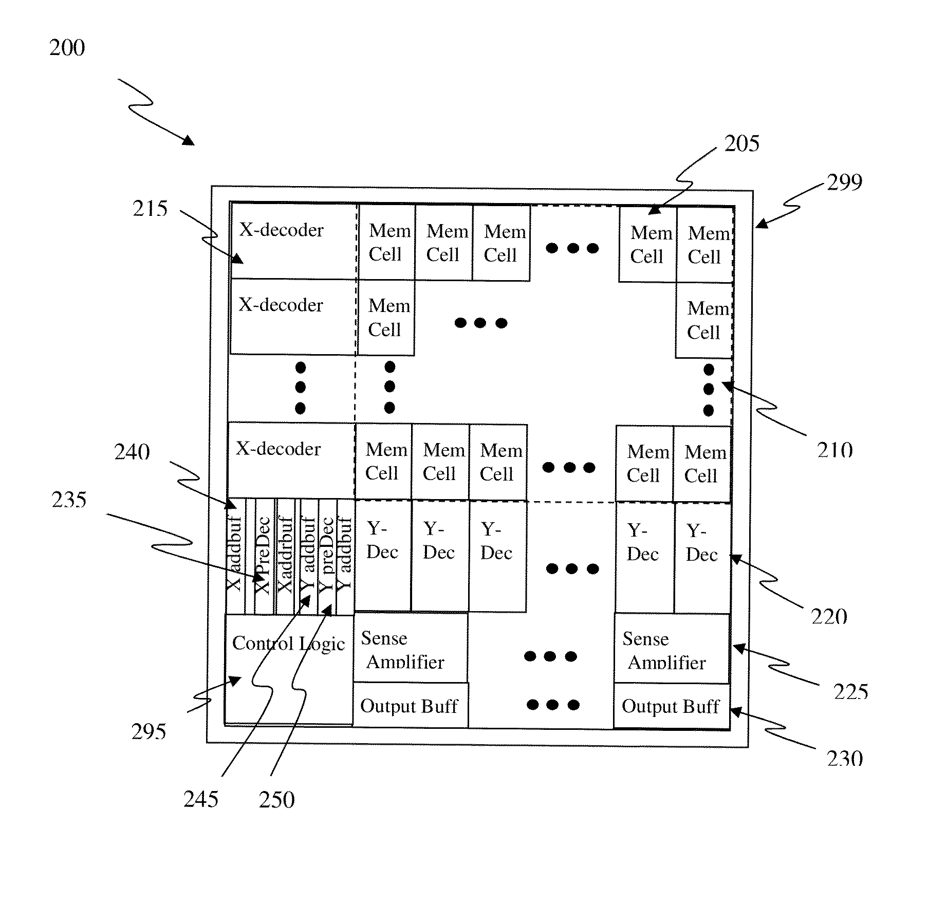
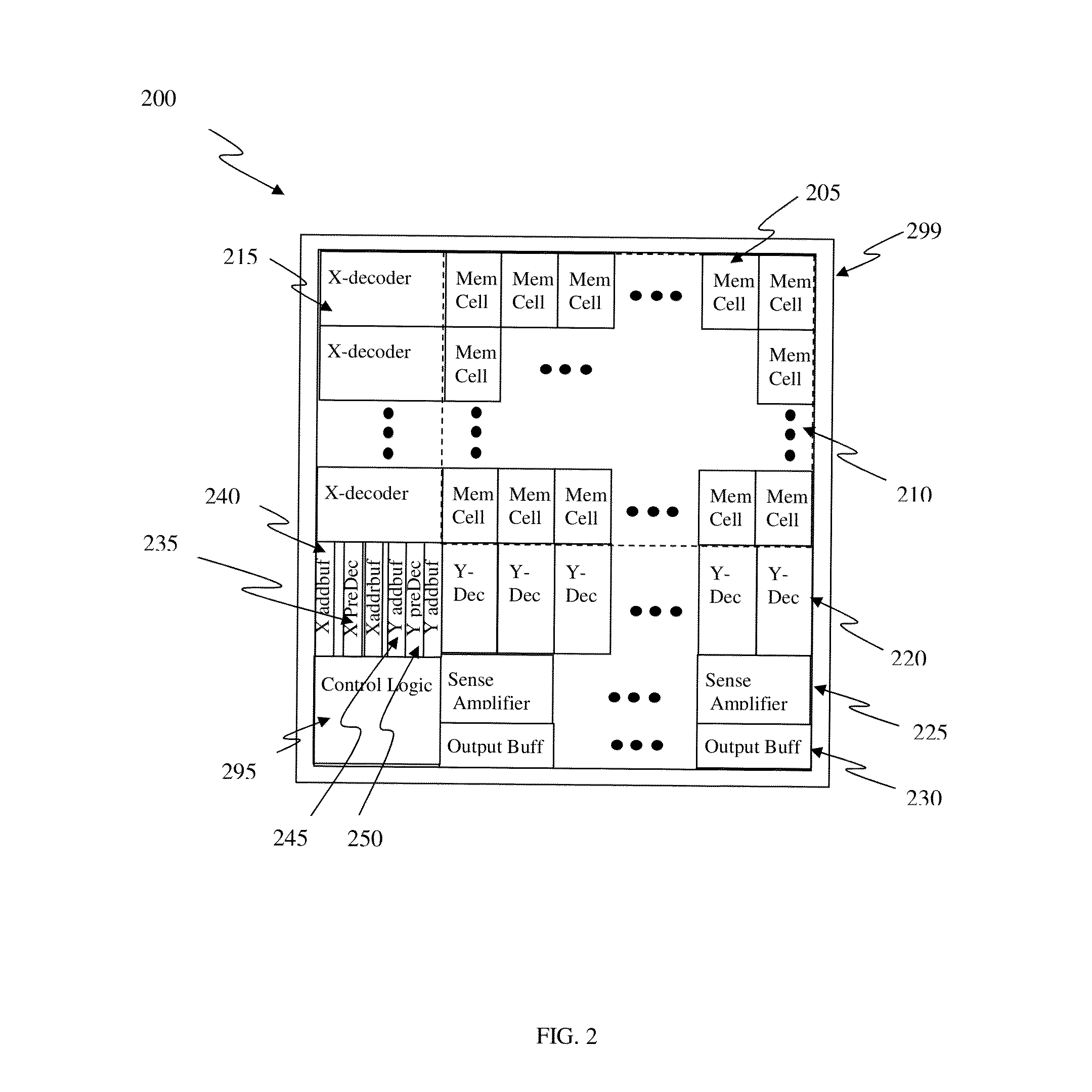
[0040]This invention is about a memory compiler based on subtractive method that can be applied to any kinds of memory. By building a full-function memory with maximum capacity as a template, smaller size memories can be generated by reducing the memory array size and the associated tight-pitch cells accordingly. The memory macro boundary can also be stretched to fit into the new floor plan of the smaller memory. Some addresses would be disabled in the new and smaller size memories. This compiler method can be applied to any memories with more components and complicated circuits, though an OTP compiler is used as an example to illustrate the key concept of this invention.

[0041]FIG. 6(a) shows a layout floor plan of a memory 200. The memory 200 has an array of n×m memory cells 205 organized in a two-dimensional array 210. An array of n X-decoders 215 are placed and butted to the memory array 210 in the left. Another array of m Y-decoders 220 are placed and butted to the memory array ...


PUM


Abstract

A memory compiler to generate a set of memories is based on a subtraction approach from a set of templates (memory templates), including at least one layout database and auxiliary design databases, by software. The software can be based on general-purpose programming language or a layout-specific language. The compiled memories can be generated by reducing the memory array sizes in row and / or column directions by moving, deleting, adding, sizing, or stretching the layout objects, and disabling the high order addresses, etc. from the memory template by software. The new auxiliary design databases, such as layout phantom, behavior model, synthesis view, placement-and-routing view or datasheet, can also be generated by modifying some parameters from the memory template by software. One-time programmable memory using junction diode, polysilicon diode, or isolated active-region diode as program selector in a cell can be generated accordingly.

Description

CROSS-REFERENCE TO RELATED APPLICATIONS[0001]This application claimed priority benefit of U.S. Provisional Patent Application No. 61 / 443,172 filed on Feb. 15, 2011, titled “Circuit and Method of a One-Time Programmable Memory Compiler Based on Subtraction Approach”, which is hereby incorporated herein by reference.[0002]This application also references U.S. Provisional Patent Application No. 61 / 375,653, filed on Aug. 20, 2010 and entitled “Circuit and System of Using Junction Diode As Program Selector for Resistive Devices in CMOS Logic Processes,” which is hereby incorporated herein by reference; U.S. patent application Ser. No. 13 / 026,725 filed on Feb. 11, 2011 based on the same title, which is hereby incorporated herein by reference; U.S. Provisional Patent Application No. 61 / 375,660, filed on Aug. 20, 2010 and entitled “Circuit and System of Using Polysilicon Diode As Program Selector for Resistive Devices in CMOS Logic Processes,” which is hereby incorporated herein by referenc...

Claims


Application Information

Patent Timeline
Patent Type & Authority Patents(United States)
IPC IPC(8): G06F13/28
CPCG06F17/5045G06F30/30
Inventor CHUNG, SHINE C.
Owner ATTOPSEMI TECH CO LTD
Why Eureka
Try Eureka