Microphone

a microphone and microphone technology, applied in the field of microphones, can solve the problems of difficult to reduce the occupying area, difficult to miniaturize the microphone, and reduce the sensitivity, and achieve the effect of small mounting area

Active Publication Date: 2013-12-31
MMI SEMICON CO LTD
View PDF11 Cites 11 Cited by
  • Summary
  • Abstract
  • Description
  • Claims
  • Application Information

AI Technical Summary

Benefits of technology

[0009]This is a configuration for a case where the circuit element and the microphone chip are mounted on the inner surface of the cover with the microphone chip mounted on the circuit element. In the first microphone of one or more embodiments of the present invention, the microphone can be miniaturized by effectively using the vertical space in the package because the circuit element and the microphone chip are accommodated in the package with the microphone chip stacked on the circuit element. In particular, the bottom area of the package can be reduced compared to the case where the circuit element and the microphone chip are arranged side by side, so that the mounting area of the microphone can be reduced. Furthermore, the performance of the microphone does not lower because the microphone chip and the circuit element themselves do not need to be reduced in size to miniaturize the microphone.
[0029]Further, in such an aspect, the acoustic perforation may be bent so that the opening on the inner surface side of the substrate cannot be linearly viewed from the opening on the outer surface side of the substrate. According to such an acoustic perforation, foreign substances can be prevented from entering the package or the microphone chip from the acoustic perforation, and environmental factors such as light or moisture can be prevented from entering from the acoustic perforation so that the microphone chip and the circuit element are less likely to be affected.

Problems solved by technology

However, in all the MEMS microphones described in U.S. Pat. No. 7,166,910, it is difficult to miniaturize the microphone and in particular, it is difficult to reduce the occupying area at the time of mounting (hereinafter referred to as the mounting area) because the microphone chip and the circuit element are arranged side by side on the upper surface of the substrate or the lower surface of the cover.
It is effective to miniaturize the microphone chip and the circuit element themselves in order to miniaturize the microphone, but the sensitivity lowers if the microphone chip is miniaturized.
Therefore, it is desired to reduce the dimension while maintaining the properties and to reduce the mounting area in the microphone, but these are difficult in conventional microphones.

Method used


Image

  • Microphone
  • Microphone
  • Microphone

Examples


first embodiment

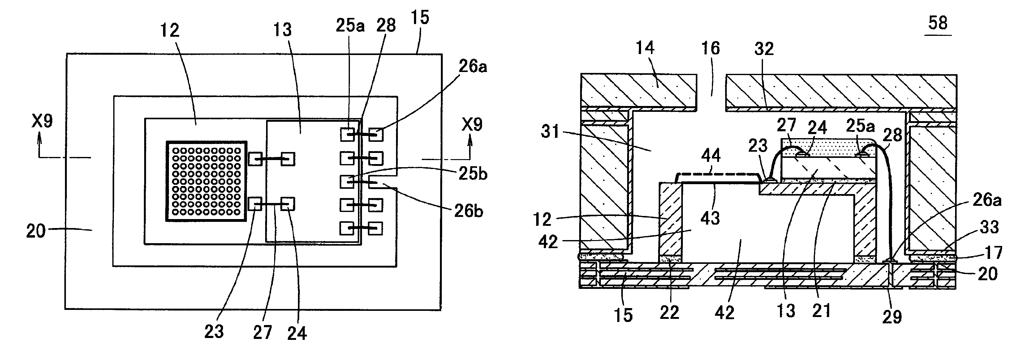
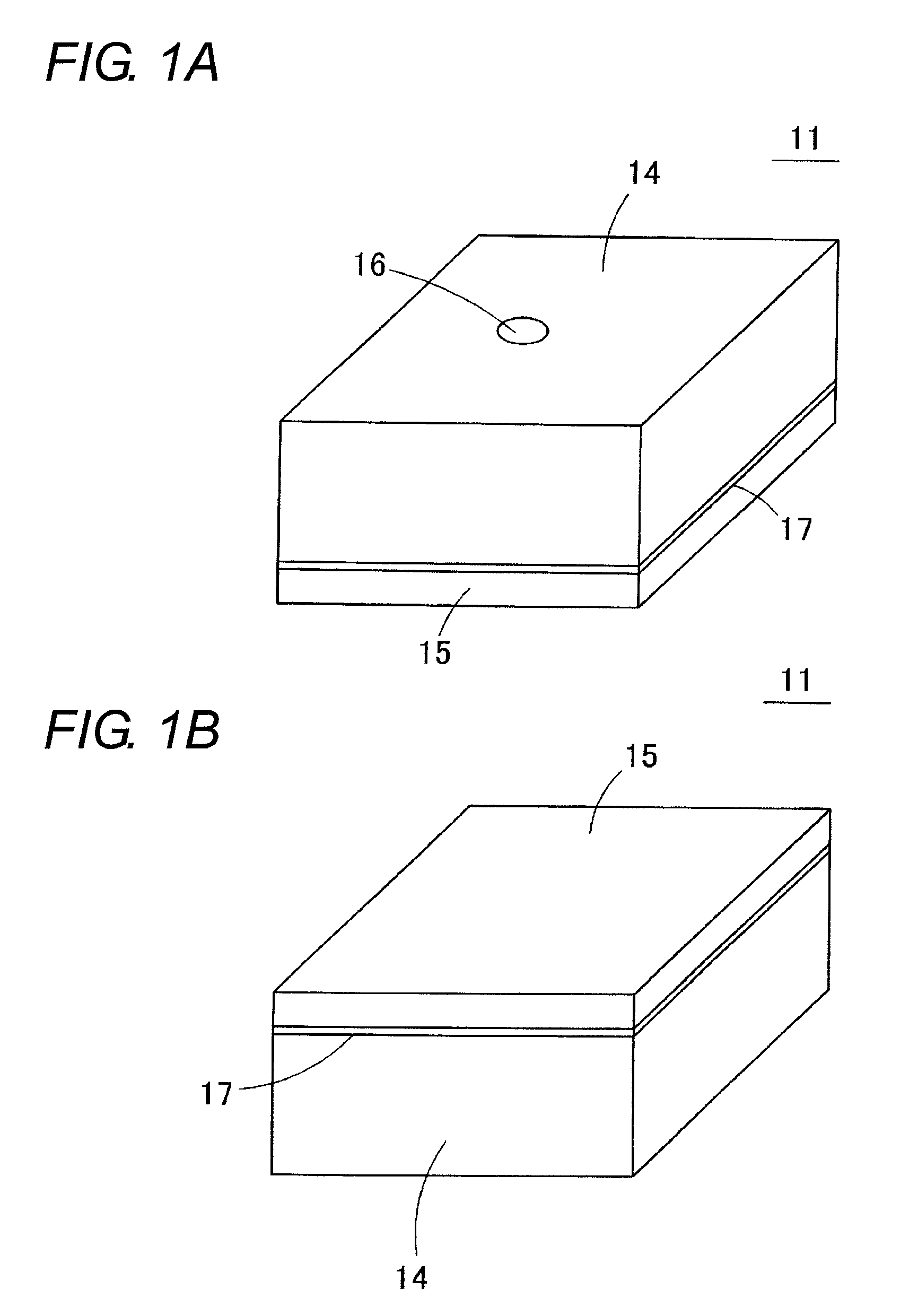
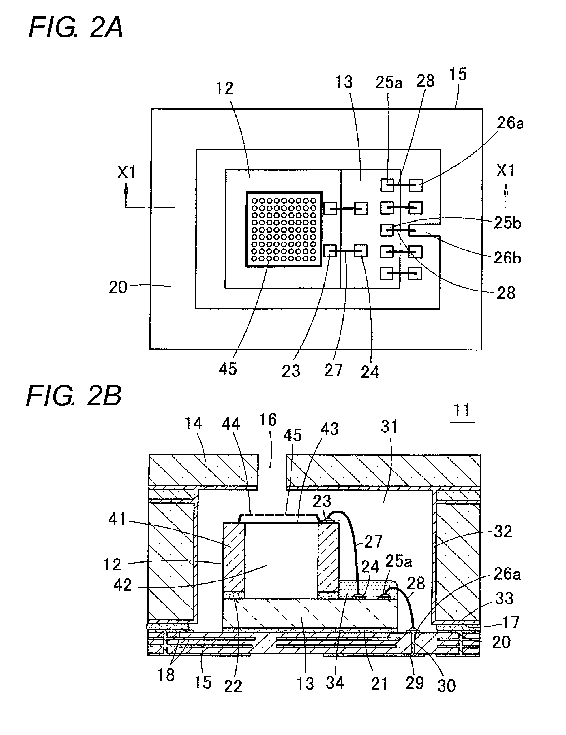
[0050]An upper surface sound hole type microphone 11 according to a first embodiment of the present invention will be described with reference to FIGS. 1A and 1B, and FIGS. 2A and 2B. FIGS. 1A and 1B are a perspective view from an upper surface side and a perspective view from a lower surface side of the microphone 11 according to the first embodiment. FIG. 2A is a plan view of a substrate 15 on which a microphone chip 12 and a circuit element 13 are mounted, and FIG. 2B is a cross-sectional view of the microphone 11 taken along an area corresponding to line X1-X1 in FIG. 2A. Such a microphone 11 is a MEMS microphone manufactured using the MEMS technique, where the microphone chip 12 and the circuit element 13 are accommodated in a package made from a cover 14 (one of a cover or a substrate) and a substrate 15 (other one of the cover or the substrate). The structure of the microphone 11 will be specifically described below.

[0051]As shown in FIGS. 2A and 2B, the substrate 15 is forme...

second embodiment

[0062]FIGS. 3A and 3B are a perspective view from an upper surface side and a perspective view from a lower surface side of a microphone 51 according to a second embodiment of the present invention. FIG. 4A is a plan view of a substrate 15 on which a microphone chip 12 and a circuit element 13 are mounted, and FIG. 4B is a cross-sectional view of the microphone 51 taken along an area corresponding to line X2-X2 in FIG. 4A.

[0063]The microphone 51 of the second embodiment differs from the microphone 11 of the first embodiment in that the acoustic perforation 16 is arranged not in the cover 14 but at a position deviated from the circuit element 13 in the substrate 15. In particular, the acoustic perforation 16 is opened at a position adjacent to the circuit element 13 to miniaturize the microphone 51. The structure substantially similar to the microphone 11 of the first embodiment is adopted for other aspects, and thus the same reference numerals are denoted for the same configuring po...

third embodiment

[0064]A microphone 52 according to a third embodiment of the present invention will now be described. FIG. 5A is a bottom view of the cover 14 on which the microphone chip 12 and the circuit element 13 are mounted in the microphone 52 of the third embodiment, and FIG. 5B is a cross-sectional view of the microphone 52 taken along an area corresponding to line X3-X3 in FIG. 5A.

[0065]In the microphone 52 of the third embodiment, the circuit element 13 and the microphone chip 12 are installed on the lower surface of the cover 14 while being turned upside down. In other words, the circuit element 13 is installed on the top surface in the recess 31 of the cover 14 by the die attach material 21 while being turned upside down. The microphone chip 12 is fixed to the lower surface of the circuit element 13 by the die attach material 22 while being turned upside down. A plurality of pad portions 26c is arranged on the lower surface of the cover 14 while being electrically insulated with the co...


PUM


Abstract

A miniaturized microphone maintaining the properties of a microphone chip and achieving a smaller mounting area. The microphone includes a package which includes a first and second member. At least one of the first second members includes a recess. The microphone also includes a circuit element installed on an inner surface of the first member. Additionally, the microphone includes a microphone chip arranged on a surface on an opposite side of an installing surface of the circuit element.

Description

BACKGROUND OF THE INVENTION[0001]1. Technical Field[0002]One or more embodiments of the present invention relate to microphones, and specifically, to a microphone in which a microphone chip (acoustic sensor) is accommodated in a package.[0003]2. Related Art[0004]For example, U.S. Pat. No. 7,166,910 describes a MEMS (Micro Electro Mechanical Systems) microphone manufactured using the MEMS technique. In the microphone described in FIG. 1 of U.S. Pat. No. 7,166,910, a package is configured by a substrate and a cover, a microphone chip and a circuit element are arranged side by side on an upper surface of the substrate, and an acoustic perforation is opened in the cover. Furthermore, in the microphone described in FIG. 31 of U.S. Pat. No. 7,166,910, the microphone chip and the circuit element are arranged side by side on the upper surface of the substrate, and the acoustic perforation is opened in the substrate at the lower surface of the microphone chip. Moreover, in the microphone des...

Claims


Application Information

Patent Timeline
Patent Type & Authority Patents(United States)
IPC IPC(8): H04R17/02H04R19/04H04R21/02H04R25/00H04R9/08H04R11/04
CPCH01L2924/3025H04R19/005H04R1/04H01L2224/48091H01L2224/73265H01L2224/49175H01L2924/1461H01L2224/05554H01L2224/48145H01L2224/8592H01L2924/15151H01L2924/16151H01L2924/16195H01L2924/00014H01L2924/00H01L2924/00012H04R19/04H01L23/12
Inventor MAEKAWA, TOMOFUMIKURATANI, NAOTOHAMAGUCHI, TSUYOSHI
Owner MMI SEMICON CO LTD
Why Eureka
Try Eureka