Array element circuit and active matrix device

a technology of active matrix and array elements, which is applied in the field of digital microfluidics, can solve the problems of not having an integrated solution with external sensor electronics, limited number of array elements at which impedance can be sensed, and insufficient ewod programming voltage (20-60v) to achieve the maximum voltage rating of tfts fabricated in standard display manufacturing processes

Active Publication Date: 2014-02-18
SHARP LIFE SCI EU LTD
View PDF31 Cites 153 Cited by
  • Summary
  • Abstract
  • Description
  • Claims
  • Application Information

AI Technical Summary

Benefits of technology

[0058]By measuring the impedance of a given droplet, it is possible to determine the size of the droplet. An impedance sensor capability can thus be used for metering quantities of fluids used in chemical and / or biochemical reactions.
[0063]By integrating sensor drive circuitry and output amplifiers into the AM-EWOD drive electronics, the impedance can be measured at a large number of points in an array with only a small number of connections being required to be made between the AM-EWOD device and external drive electronics. This improves manufacturability and minimises cost compared to a passive matrix sensor arrangement, as in the prior art, where the impedance at each location in the array has to be connected individually.
[0064]An integrated impedance sensor capability requires few or no additional process steps or assembly cost in comparison to a standard AM-EWOD device.
[0066]Only certain less performance-critical circuit components are required to withstand high voltages such as are required for the EW-drive voltage. This reduces layout footprint, improves reliability and improves circuit performance.

Problems solved by technology

However a disadvantage of this method is that the number of array elements at which impedance can be sensed is limited by the number of connections that can be supplied to the device.
Furthermore this is not an integrated solution with external sensor electronics being required.
However the large AM-EWOD programming voltages (20-60V) can in some instances still exceed the maximum voltage ratings of TFTs fabricated in standard display manufacturing processes.
However such modifications to device design may impair the TFT performance.
The effects of this are particularly deleterious for devices which are required to operate at high speed or to perform analogue circuit functions.
A disadvantage of the above circuit is that there is no provision of any DC current path to the sense node 102.
The small LC capacitance also makes changes difficult to sense.
A disadvantage of MOS capacitors is that the capacitance becomes a function of the terminal biases if the potentials are not arranged so that the channel semiconductor material is completely in accumulation. FIG. 17 shows at 124 the typical characteristics of a MOS capacitor 120 where the semiconductor material 122 is doped n-type.

Method used


Image

  • Array element circuit and active matrix device
  • Array element circuit and active matrix device
  • Array element circuit and active matrix device

Examples


first embodiment

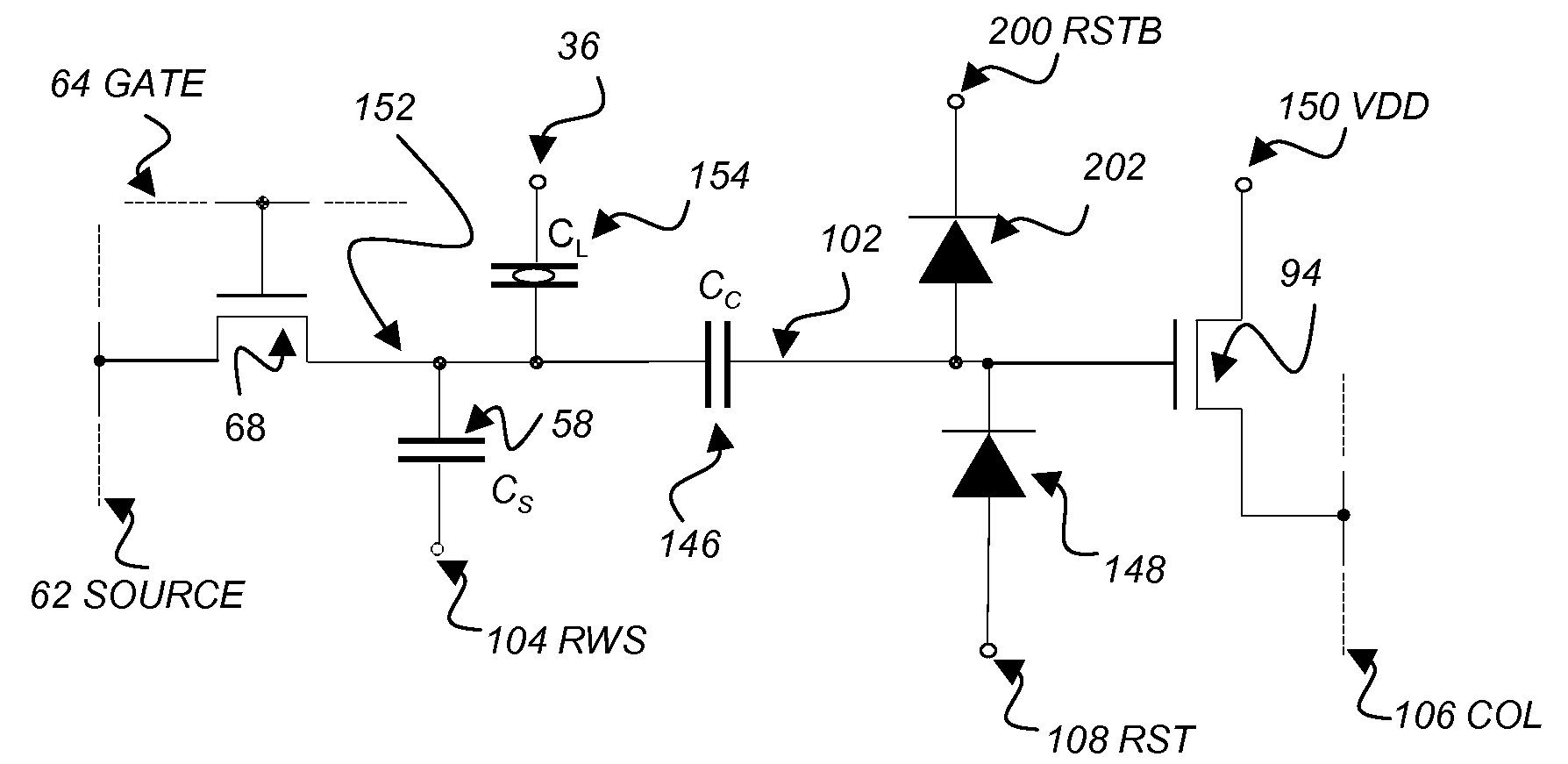
[0222]The first embodiment is shown in FIG. 24. This consists of an array element circuit for an AM-EWOD device with integrated impedance sensor. As with each of the embodiments of the invention described herein, a plurality of the described array elements are included in an AM display in an array of rows and columns with corresponding driver circuits similar to FIG. 13. Accordingly, additional detail regarding the otherwise conventional portions of the display have been omitted for sake of brevity.

[0223]Referring again to FIG. 24, the array element circuit includes the following elements:[0224]A switch transistor 68[0225]A capacitor CS 58[0226]A coupling capacitor CC 146[0227]A diode 148[0228]A diode 202[0229]A transistor 94

Connections supplied to the array element are as follows:[0230]A source addressing line 62 which is shared between array elements in the same column[0231]A gate addressing line 64 which is shared between array elements in the same row[0232]A sensor row select li...

fourth embodiment

[0274]The fourth embodiment is shown in FIG. 27.

[0275]This embodiment is as the first embodiment FIG. 24 except that the diodes 148 and 202 have been removed and the following additional array elements have been added[0276]A p-type transistor 205[0277]An n-type transistor 206[0278]A power supply line VRST 208 which may be common to all elements in the array.

[0279]The reset line RST 108 is connected to the gate of transistor 206. The reset line RSTB 200 is connected to the gate of transistor 205. The source of transistors 205 and 206 are connected together and to the sense node 102. The drain of transistors 205 and 206 are connected together and to the power supply line VRST 208.

[0280]The operation of this embodiment is as described for the first embodiment in FIG. 24 except in the performance of the reset operation. In this embodiment reset is performed by taking the reset line RST 108 to a logic high level and the reset line RSTB 200 to a logic low level. This has the effect of tur...

second embodiment

[0292]The operation of the circuit is essentially similar to that of the second embodiment with the exception that the bias supply VBR 172 is maintained at a bias VX below that of the bias voltage of the sensor row select line RWS 104 throughout the operation of the circuit. This has the effect of making the gated P-I-N diode 144 function like a voltage dependent capacitor, having a bias dependence that is a function of VX, as described in prior art.

[0293]By choosing the range of operation of the RWS pulse high and low levels and an appropriate value of VX it is therefore possible to make the gated P-I-N diode 144 function as a variable capacitor whose value depends upon the choice of VX. The overall circuit functions as described in the second embodiment, where the gated P-I-N diode 144 is a capacitor whose capacitance can be varied. The circuit can therefore effectively operate in different ranges according to whether this capacitance is arranged to take a high or a low value

[0294...


PUM


Abstract

An array element circuit with an integrated impedance sensor is provided. The array element circuit includes an array element which is controlled by application of a drive voltage by a drive element; writing circuitry for writing the drive voltage to the drive element; and sense circuitry for sensing an impedance presented at the drive element.

Description

TECHNICAL FIELD[0001]The present invention relates to active matrix arrays and elements thereof. In a particular aspect, the present invention relates to digital microfluidics, and more specifically to AM-EWOD. Electrowetting-On-Dielectric (EWOD) is a known technique for manipulating droplets of fluid on an array. Active Matrix EWOD (AM-EWOD) refers to implementation of EWOD in an active matrix array, for example by using thin film transistors (TFTs).BACKGROUND ART[0002]FIG. 1 shows a liquid droplet 4 in contact with a solid surface 2 and in static equilibrium. The contact angle θ6 is defined as shown in FIG. 1, and is determined by the balancing of the surface tension components between the solid-liquid (γSL 8), liquid-gas (γLG 10) and solid gas (γSG 12) interfaces, as shown, such that:[0003]cos⁢⁢θ=γSG-γSLγLG(equation⁢⁢1)[0004]The contact angle θ is thus a measure of the hydrophobicity of the surface. Surfaces may be described as hydrophilic if θ<90 degrees or hydrophobic if θ&g...

Claims


Application Information

Patent Timeline
Patent Type & Authority Patents(United States)
IPC IPC(8): B01D57/02
CPCB01L2200/0673G09G2300/0857B01L2400/0427G09G2320/0693B01L3/50273B01L2300/0645G09G3/006G09G3/00G09G3/348B01L2300/161G09G2330/10B01L2200/061B01L2200/143G09G2300/0469
Inventor HADWEN, BENJAMIN J.HECTOR, JASON R.JACOBS, ADRIAN MARC SIMONZEBEDEE, PATRICK
Owner SHARP LIFE SCI EU LTD
Why Eureka
Try Eureka