

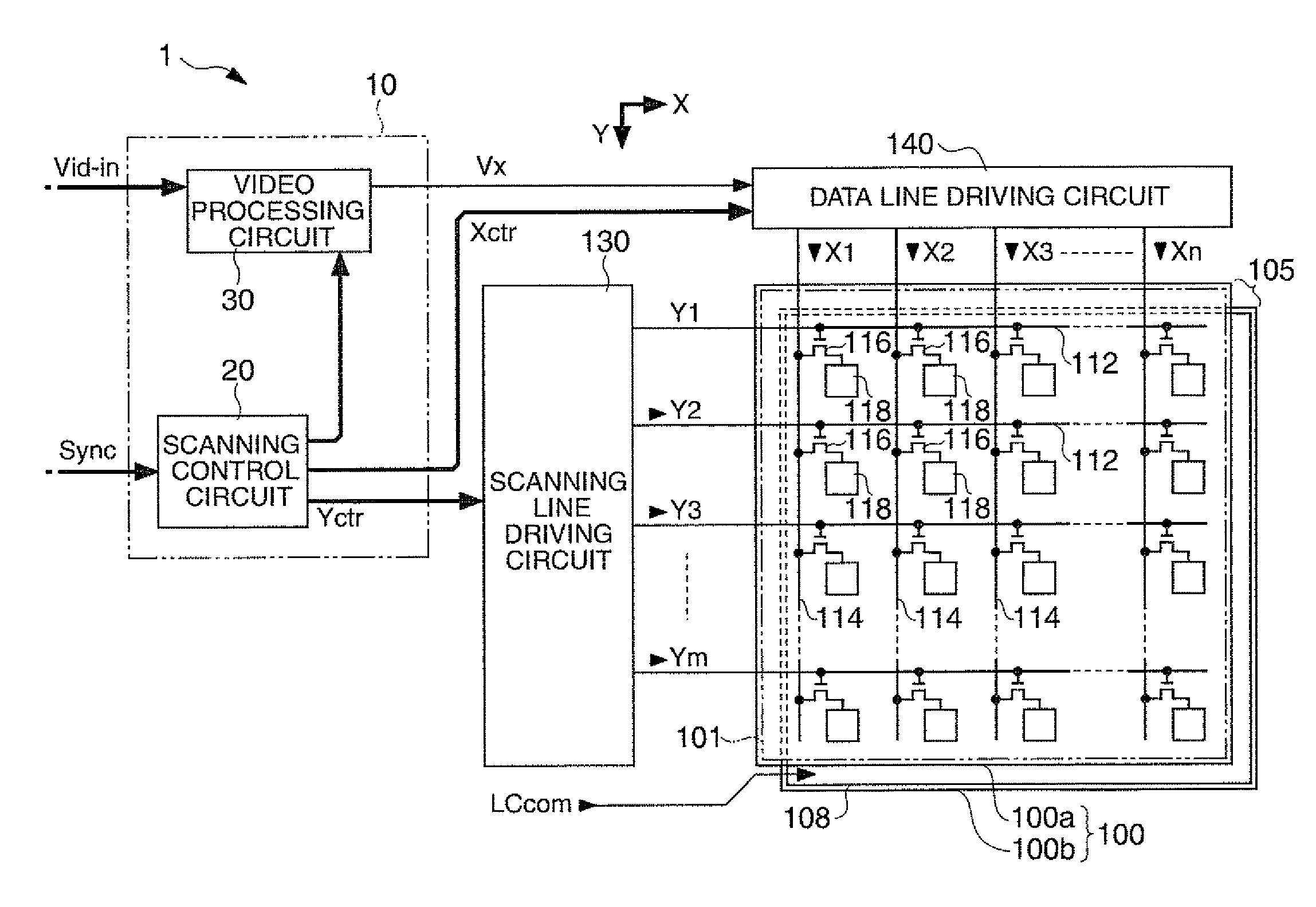
Video processing circuit, video processing method, liquid crystal display apparatus and electronic device
a liquid crystal display and video processing technology, applied in the field of video processing circuits, video processing methods, liquid crystal display apparatuses and electronic devices, can solve the problems of easy reduction of aperture ratio, display defect, and difficulty in applying the technique to an existing liquid crystal display panel without contrivance of structure, so as to reduce the reverse tilt domain
- Summary
- Abstract
- Description
- Claims
- Application Information
AI Technical Summary
Benefits of technology
Problems solved by technology
Method used
Image

Examples
example 1
Number of Pixels to be Changed
[0114]In the embodiment, only one dark pixel adjacent to the application boundary is replaced by the gray scale level “c1”. In such a configuration, in order to decrease the transverse electric field generated in the application boundary between the dark pixel and the bright pixel, it is preferable to increase the raising amount of the voltage applied to the dark pixel adjacent to the application boundary. However, if the raising amount (correction amount) of the applied voltage increases, this causes discrepancy with the original image and the display departure.
[0115]Accordingly, in a case where the dark pixels are continuous, in addition to the dark pixel adjacent to the application boundary, with respect to K dark pixels (K is an integer which is equal to or more than 1) which continue in a direction (direction perpendicular to the application boundary) away from the application boundary to the dark pixel, gray scale levels thereof may be changed.
[01...
example 2
Another Example of Application Boundary
[0120]In the embodiment, the boundary where the dark pixel of the gray scale range “a” and the bright pixel of the gray scale range “b” are adjacent to each other is detected, and the boundary which moves from the boundary prior to one frame by one pixel, within the detected boundary, is set as the application boundary. The following three patterns are considered as this application boundary, in consideration of the change to the current frame from the previous frame. That is, in a case where the dark pixel and the bright pixel are adjacent to each other in the current frame, there are three cases, that is, a case where the two pixels are all dark pixels in the previous frame (pattern 1), a case where the two pixels are all bright pixels in the previous frame (pattern 2), and a case where two pixels which have been the bright pixel and the dark pixel in the previous frame are changed to be in the opposite state in the current frame (pattern 3)....
example 3
Pixel which is Replacement Target
[0127]In the embodiment, the dark pixel is replaced by the gray scale level “c1”, among the dark pixel and the bright pixel between which the application boundary is interposed. This is because a pixel in which liquid crystal molecules are in an unstable state since the voltage applied to the liquid crystal element is low in the normally black mode is a dark pixel.
[0128]On the other hand, in order to suppress generation of the reverse tilt domain, it is effective to only reduce the transverse electric field generated in the dark pixel and the bright pixel between which the application boundary is interposed.
[0129]Here, in order to reduce the transverse electric field generated in the dark pixel and the bright pixel between which the application boundary is interposed, like the embodiment, in addition to the process of changing the dark pixel in the normally black mode into the gray scale level “c1” to correct it in a bright direction, a process of co...
PUM
 Abstract
Description
Claims
Application Information