Liquid crystal pixel correction using pixel boundary detection

boundary detection technology, applied in the field of liquid crystal pixel correction using pixel boundary detection, can solve the problems of display defect, difficult to apply the technique to a liquid crystal panel that has already been manufactured without taking

Active Publication Date: 2015-09-22
SEIKO EPSON CORP
View PDF33 Cites 0 Cited by
  • Summary
  • Abstract
  • Description
  • Claims
  • Application Information

AI Technical Summary

Benefits of technology

[0008]An advantage of some aspects of the invention is that it provides a technique that reduces the reverse tilt domain while resolving the above-described problems.
[0012]Furthermore, in the correcting of the video signal, out of two or more of the first pixels corresponding to a number defined in advance that are consecutive on a side opposite to the risk boundary from the first pixel that is brought into contact with the risk boundary detected in accordance with the video signal of the frame brought into contact with the risk boundary, the first pixel of which the application voltage is lower than a third voltage which is lower than the first voltage may be corrected such that the application voltage is equal to or higher than the third voltage. In such a case, a change in the application voltage due to the correction of the video signal may not visually noticeable. In addition, the continuation of the unstable state of the liquid crystal molecules in the next updating process (rewriting) can be suppressed.
[0015]In addition, in the correcting of the video signal, it is preferable that, out of the boundary detected in the detecting of a boundary, the pixel that is brought into contact with the risk boundary that moves by one pixel is set as a correction target for decreasing a lateral direction electric field. In such a case, the influence of the reverse tilt domain may be easily received. Furthermore, since the trailing phenomenon is intensively corrected for a visually-noticeable position, the change in the input video signal can be suppressed.

Problems solved by technology

However, in a case where the pixel pitch has become narrow due to a recent trend of reduction in size and higher precision, an electric field that is generated between pixel electrodes adjacent to each other, that is, an electric field is generated in a direction parallel to the substrate surface (lateral direction), and the effect thereof is becoming such that it is no longer negligible.
For example, if a lateral direction electric field is applied to a liquid crystal to be driven by a vertical electric field, such as a VA (Vertical Alignment) type or a TN (Twisted Nematic) type, a defect in the alignment of the liquid crystal (that is, reverse tilt domain) occurs, thereby causing a display defect.
Furthermore, there is a problem in that it is difficult to apply the technique to a liquid crystal panel that has already been manufactured without taking the structure thereof into account.
On the other hand, according to the technique of clipping a video signal having a set value or more, there is a problem in that the brightness of a displayed image is limited to the set value.
In such a case, a change in the application voltage due to the correction of the video signal may be visually unnoticeable.

Method used


Image

  • Liquid crystal pixel correction using pixel boundary detection
  • Liquid crystal pixel correction using pixel boundary detection
  • Liquid crystal pixel correction using pixel boundary detection

Examples


first embodiment

[0054]Hereinafter, embodiments of the invention will be described with reference to the accompanying drawings.

[0055]First, a first embodiment of the invention will be described.

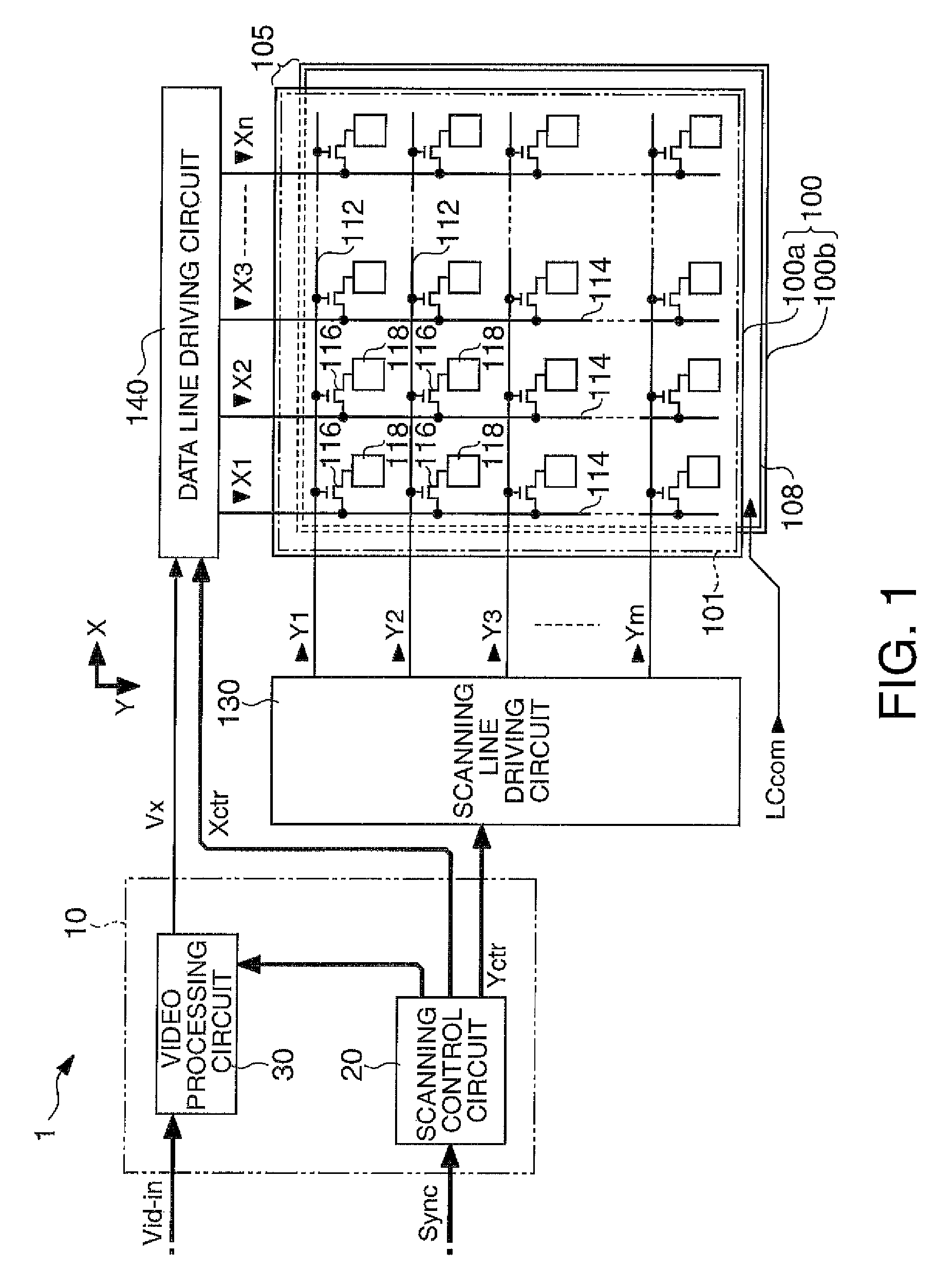
[0056]FIG. 1 is a block diagram showing the entire configuration of a liquid crystal display device 1 to which a video processing circuit according to this embodiment of the invention is applied.

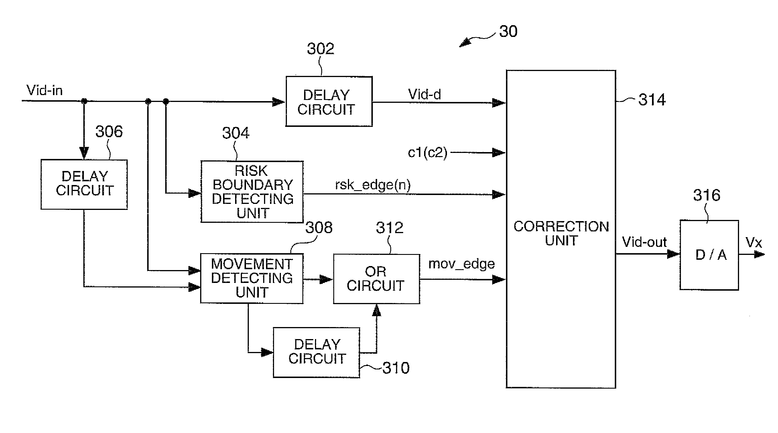
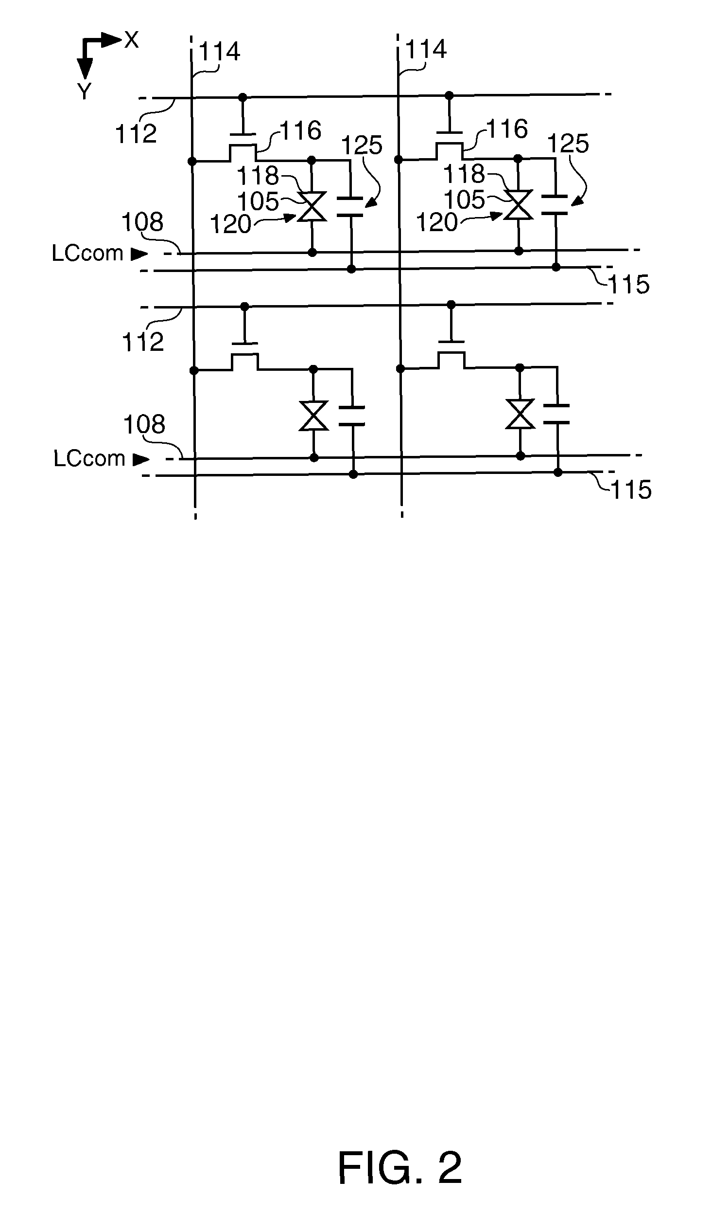
[0057]As shown in FIG. 1, a liquid crystal display device 1 includes a control circuit 10, a liquid crystal panel 100, a scanning line driving circuit 130, and a data line driving circuit 140. A video signal Vid-in is supplied to the control circuit 10 from a higher-level device in synchronization with a synchronization signal Sync. The video signal Vid-in is digital data that designates a gray scale level of each pixel in the liquid crystal panel 100 and is supplied in the scanning order based on a vertical scanning signal, a horizontal scanning signal and a dot clock signal (not shown in the figure) that are include...

second embodiment

[0175]Next, a second embodiment of the invention will be described. Further in this embodiment, the description will be presented on the premise of a normally black mode. This applies the same to each embodiment described below unless otherwise described. In addition, in the description presented below, the same reference numeral is assigned to the same configuration as that of the first embodiment, and the detailed description thereof will be appropriately omitted. In the above-described first embodiment, the video processing circuit 30 corrects only the dark pixels satisfying the correction condition to the gray scale level c1. However, in this embodiment, two or more dark pixels that are consecutive from a dark pixel, which is brought into contact with a risk boundary, to the opposite side of the risk boundary are also set as the correction targets that are corrected to the gray scale level c1.

[0176]As above, a difference between a video processing circuit 30 according to this em...

third embodiment

[0185]Next, a third embodiment of the invention will be described.

[0186]In this embodiment, in the configuration according to the first embodiment, instead of dark pixels satisfying the correction condition, the video signals of bright pixels satisfying the correction condition are corrected. In this embodiment, correction of dark pixels is not performed. Accordingly, in this embodiment, instead of raising the gray scale levels of dark pixels so as to suppress “(3) the state in which the liquid crystal molecules in the pixels, which are changed to bright pixels in frame n, are unstable in frame (n−1) that is one frame before” described above, the lateral direction electric field is suppressed focusing on the condition that “(1) when frame n is considered, a dark pixel and a bright pixel are adjacent to each other, in other words, a pixel to which a low voltage is applied and a pixel to which a high voltage is applied are adjacent to each other, and the lateral direction electric fie...


PUM


Abstract

A video processing circuit detects a risk boundary that is a part of a boundary between a dark pixel and a bright pixel, and is determined in accordance with the tilt azimuth of liquid crystal molecules from a boundary changed over the previous frame to the current frame and, for at least one side of dark pixels and bright pixels brought into contact with the detected risk boundary, corrects a video signal designating the application voltage of a liquid crystal element corresponding to the pixel of the frame brought into contact with the risk boundary out of a plurality of frames from the current frame to k frames (here, k is a natural number) following the current frame such that a lateral direction electric field generated between the dark pixel and the bright pixel decreases.

Description

BACKGROUND[0001]1. Technical Field[0002]The present invention relates to a technique for reducing display defects on a liquid crystal panel.[0003]2. Related Art[0004]A liquid crystal panel has a configuration in which a liquid crystal is interposed between one pair of substrates maintained so as to be separated from each other by a constant gap. Described in detail, the liquid crystal panel has a configuration in which pixel electrodes for pixels are arranged in a matrix pattern on one substrate, a common electrode is disposed so as to be common to the pixels on the other substrate, and a liquid crystal is interposed between the pixel electrodes and the common electrode. When a voltage according to a gray scale level is applied and maintained between the pixel electrode and the common electrode, the alignment state of the liquid crystal is defined for each pixel, and thereby the transmittance or the reflectance is controlled. Thus, in the above-described configuration, only a compon...

Claims


Application Information

Patent Timeline
Patent Type & Authority Patents(United States)
IPC IPC(8): G09G3/36
CPCG09G3/3648G09G2320/0209G09G2320/10G09G2340/16
Inventor HOSAKA, HIROYUKIKITAGAWA, TAKU
Owner SEIKO EPSON CORP
Why Eureka
Try Eureka