Methods and systems for maintaining cache coherency in multi-processor systems
a multi-processor system and cache technology, applied in the field of spinlock method, can solve the problems of difficult selection of optimal wait time, vain consumption of processor power, and deterioration of spinlock performance, so as to reduce power consumption at the time of executing a spin wait loop
- Summary
- Abstract
- Description
- Claims
- Application Information
AI Technical Summary
Benefits of technology
Problems solved by technology
Method used
Image
Examples
first embodiment
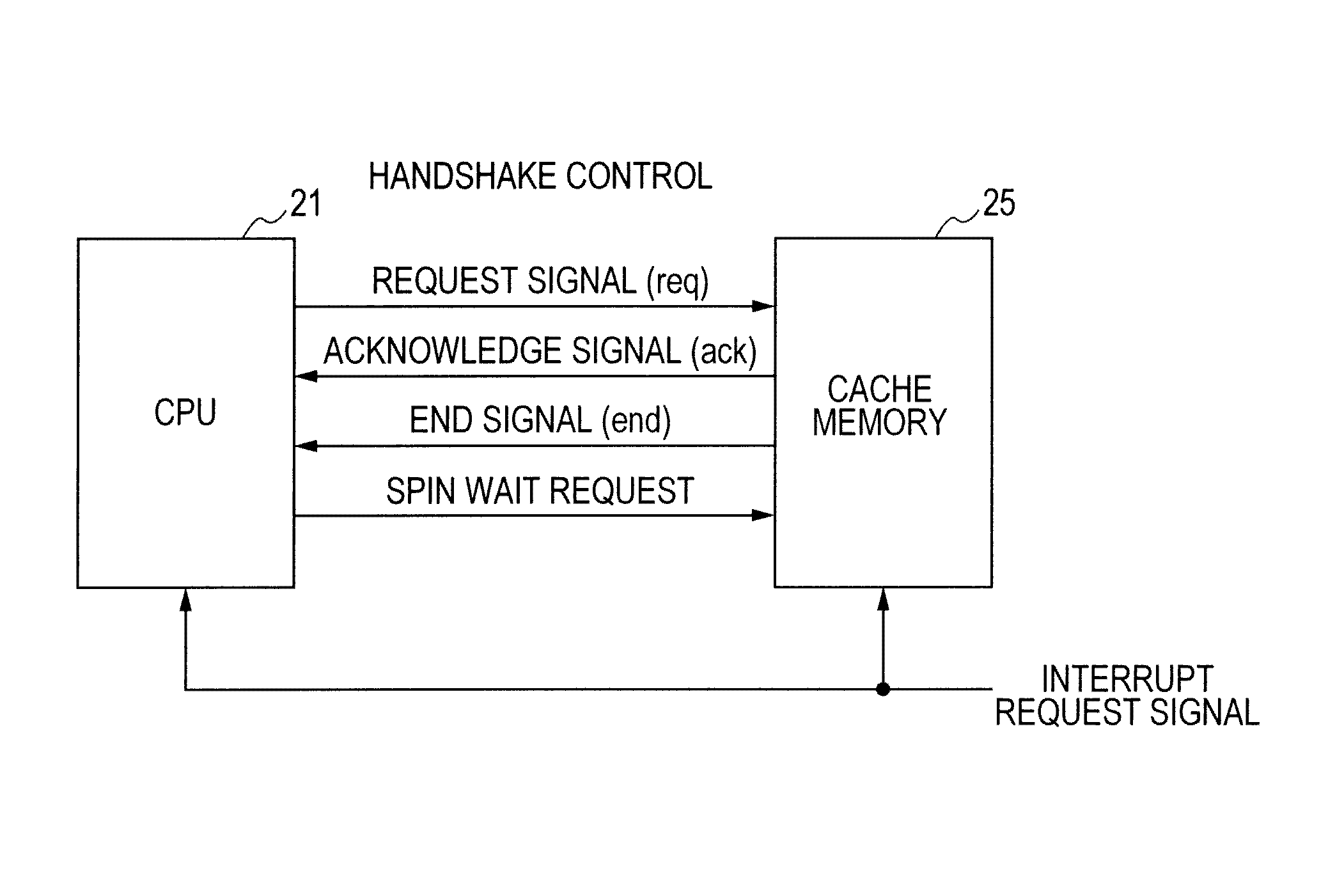
[0073]FIG. 6 is a diagram showing an example of connection between the CPU 21 and the cache memory 25 in the data processor according to the first embodiment of the invention. The CPU 21 and the cache memory 25 are coupled by handshake signals such as a request (req) signal, an acknowledge (ack) signal, and an end signal. By performing the handshake control by the CPU 21, a memory access process is performed with reliability.
[0074]The CPU 21 outputs a spin wait request signal to the cache memory 25 at the time of executing a weighted load instruction (LDS instruction) or a spin wait instruction (SPIN instruction) which will be described later. To the cache memory 25, an interrupt request signal is coupled. The details of them will be described later.
[0075]FIG. 7 is a block diagram showing a configuration example of the CPU 21 in the data processor in the first embodiment of the invention. The CPU 21 includes an instruction fetch unit 31, an instruction decode unit 32, a control unit...
second embodiment
[0130]In the data processor in the first embodiment, when the CPU 21 executes the weighted load instruction, the CPU 21 transmits a spin wait request to the cache memory 25 to make the cache memory 25 enter the spin wait state. A data processor in a second embodiment is different from the data processor in the first embodiment only with respect to the point that a spin wait (SPIN) instruction is provided for the CPU 21, and the CPU 21 continuously holds the instruction until a load result becomes a designated value. Therefore, the detailed description of configurations and functions will not be repeated.
[0131]FIG. 17 is a diagram showing an example of a spinlock process code executed by the CPU 21 in the second embodiment of the invention. The spinlock process code is different from that of FIG. 10 only with respect to the point that a weighted load instruction (LDS instruction) and a bgtz instruction are replaced with a spin wait instruction (SPIN instruction).
[0132]The instruction...
third embodiment
[0140]A data processor in a third embodiment of the invention is different from the data processors in the first and second embodiments only with respect to the point that a mode of supplying clocks to the CPU 21 and the cache memory 25 is changed interlockingly with shift to the spin wait state and return from the spin wait state. Therefore, the detailed description of configurations and functions will not be repeated.
[0141]FIG. 19 is a block diagram showing a configuration example of the data processor in the third embodiment of the invention. The data processor is obtained by adding a clock module (CLKC) 27 to the data processor in the first embodiment shown in FIG. 6.
[0142]The cache memory 25 is divided into a part which operates in a CPU clock domain and a part which operates in a cache clock domain. At the time of shift to the spin wait state, the cache memory 25 notifies the clock module 27 of the fact that the cache memory 25 is in the spin wait state and makes the clock mod...
PUM
 Abstract
Description
Claims
Application Information


