Method of forming nano dots, method of fabricating the memory device including the same, charge trap layer including the nano dots and memory device including the same
a memory device and nano-dot technology, applied in the field of semiconductor memory devices, can solve the problems of non-volatile memory devices, random access memory (drams), and loss of stored data, and achieve the effect of preventing or reducing the degradation of the memory characteristic of nano-dots
- Summary
- Abstract
- Description
- Claims
- Application Information
AI Technical Summary
Benefits of technology
Problems solved by technology
Method used
Image
Examples
experimental example 1
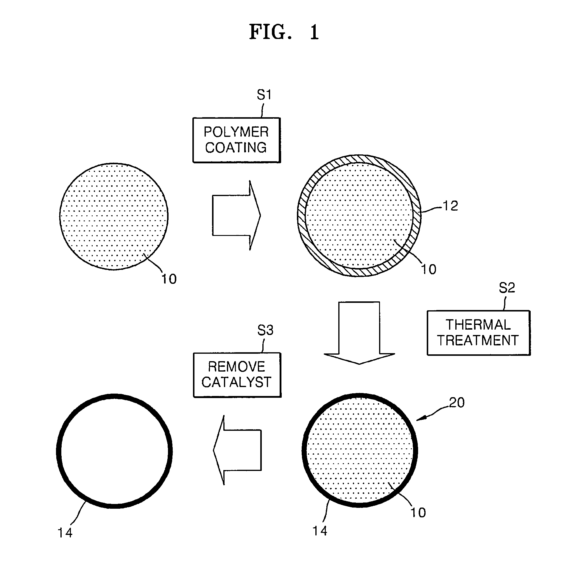
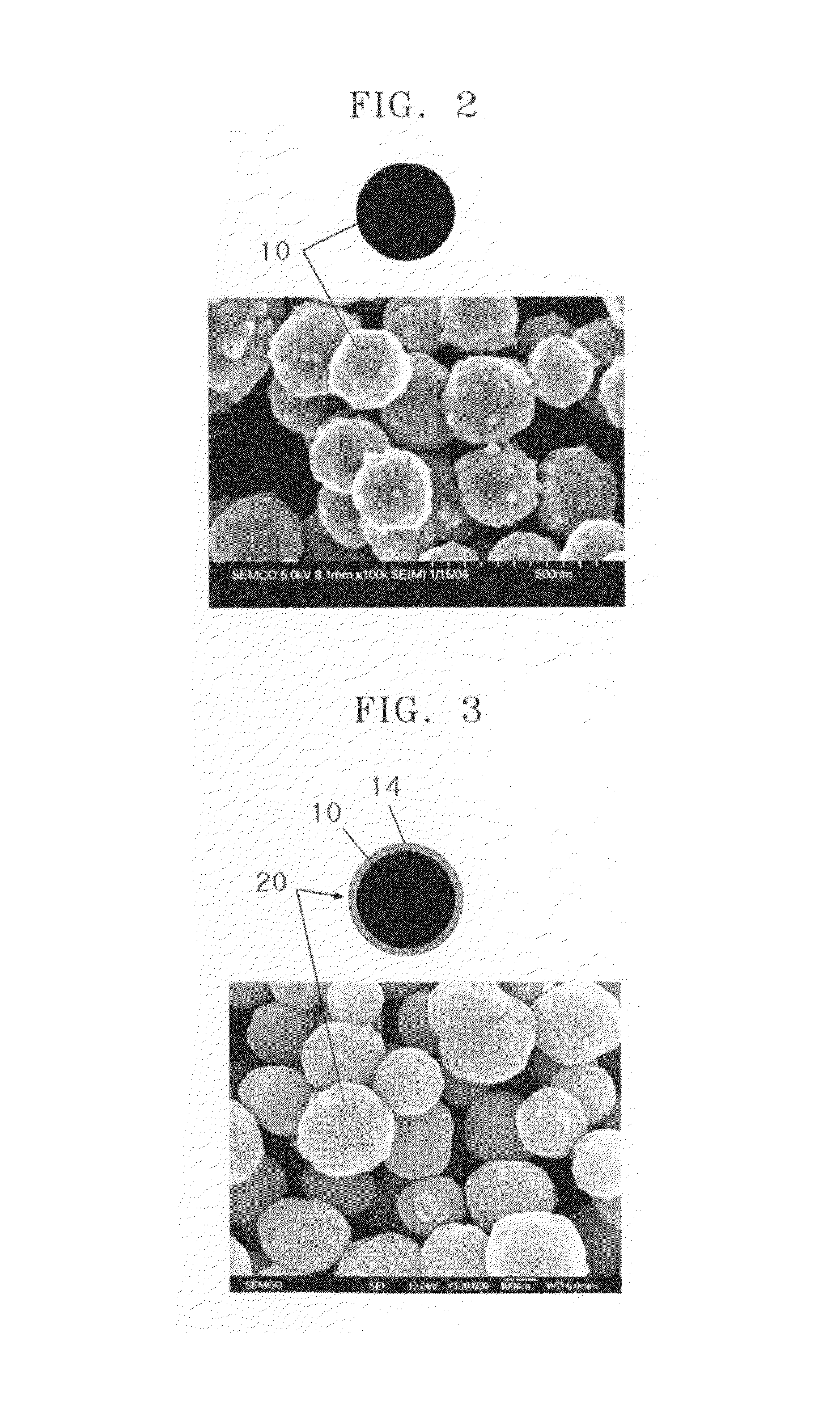
[0045]1. About 20 Kg of Ni particles, each having a diameter of about 300 μm, was input into about 120 kg of water, and then, the water was agitated for about one hour at about 400 rpm.[0046]2. A solution, which was made by mixing about 1 kg of oleic acid into about 46.7 kg of water, was input into the first agitated solution, and then, the mixed solution was agitated for about five hours at about 400 rpm.[0047]3. After the second agitation, a Ni powder solution, on which a polymer was coated, was input into a filter paper under vacuum atmosphere to remove the water from the Ni powder solution. Then, Ni powder coated with the polymer was obtained.[0048]4. The obtained Ni powder was heated for about twelve hours at a temperature of about 60° C. under a vacuum atmosphere to remove water remaining on surfaces of the coated Ni powder.[0049]5. After the drying process, the Ni powder coated with the polymer was thermally treated at a temperature of about 500° C. under a nitrogen atmospher...
experimental example 2
[0053]About 400 g of Oleic acid was used, and the other conditions were the same as those of the above experimental example. In the second experimental example, the graphene layer 14 having a thickness of about 2 nm was formed.
experimental example 3
[0054]About 600 g of oleic acid was used, and the other conditions were the same as those of the first experimental example. In the third experimental example, the graphene layer 14 having a thickness of about 3 nm was formed.
PUM
| Property | Measurement | Unit |
|---|---|---|
| temperature | aaaaa | aaaaa |
| diameter | aaaaa | aaaaa |
| work functions | aaaaa | aaaaa |
Abstract
Description
Claims
Application Information


