Method of forming nano dots, method of fabricating the memory device including the same, charge trap layer including the nano dots and memory device including the same

a memory device and nano-dot technology, applied in nanoinformatics, light beam reproducing, instruments, etc., can solve the problems of non-volatile memory devices, random access memory (drams), and may lose stored data, so as to prevent or reduce the memory characteristic of nano-dots from degrading

Inactive Publication Date: 2009-04-23
SAMSUNG ELECTRONICS CO LTD
View PDF10 Cites 24 Cited by
  • Summary
  • Abstract
  • Description
  • Claims
  • Application Information

AI Technical Summary

Benefits of technology

[0009]Example embodiments provide a method of forming nano dots, which may prevent or reduce a memory characteristic of nano dots from degrading due to a post thermal treatment performed on the nano dots

Problems solved by technology

However, volatile memory devices, e.g., dynamic random access memories (DRAMs), may lose the stored data when a supply of electric power is stopped.
Non-volatile memory devices may store the data for a relatively long ti

Method used


Image

  • Method of forming nano dots, method of fabricating the memory device including the same, charge trap layer including the nano dots and memory device including the same
  • Method of forming nano dots, method of fabricating the memory device including the same, charge trap layer including the nano dots and memory device including the same
  • Method of forming nano dots, method of fabricating the memory device including the same, charge trap layer including the nano dots and memory device including the same

Examples


experimental example 1

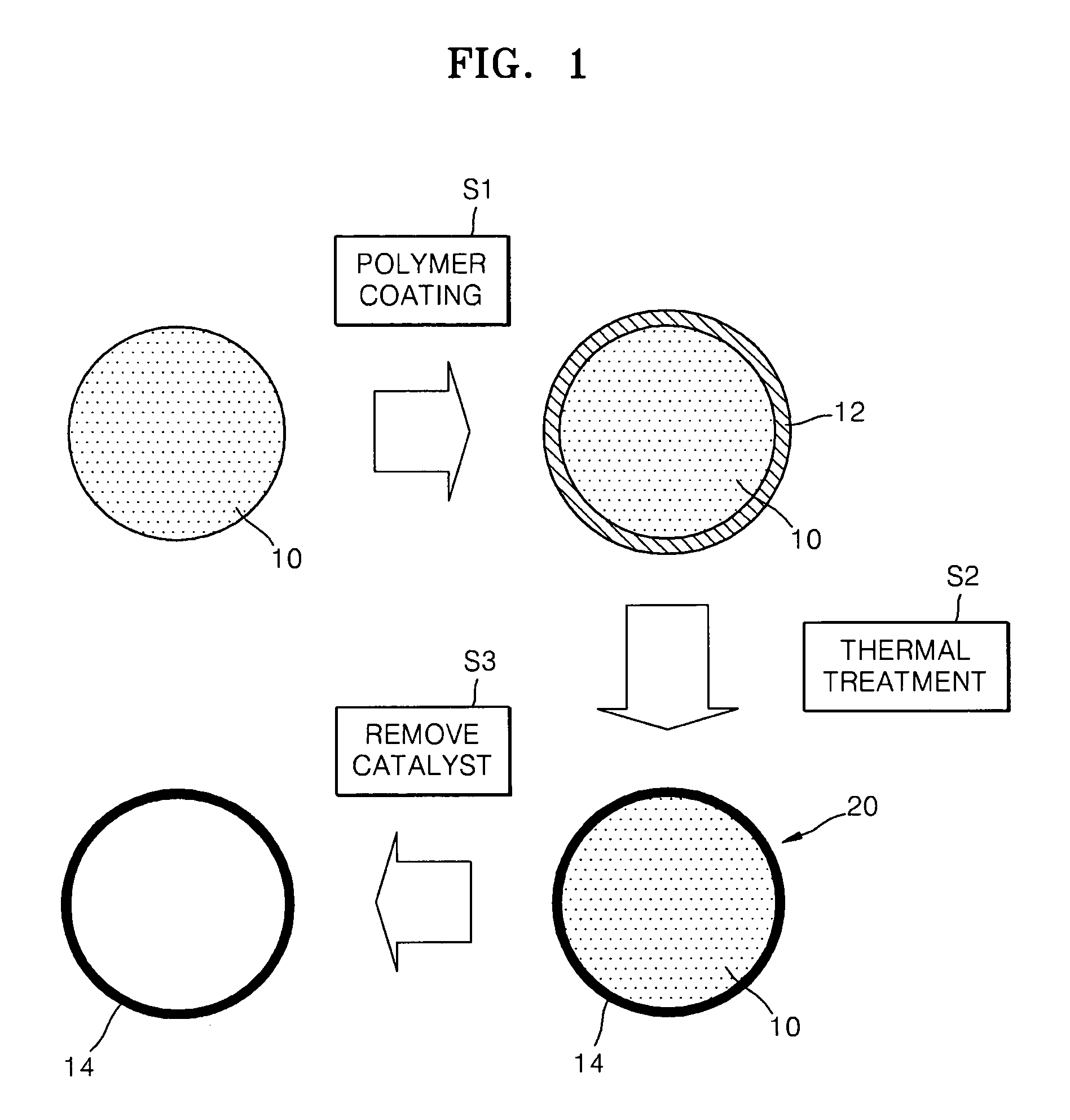
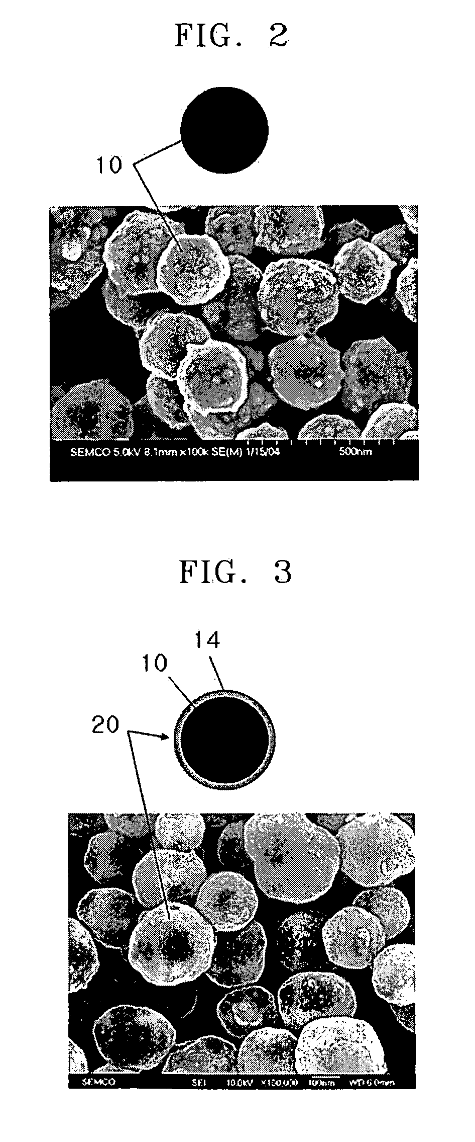
[0045]1. About 20 Kg of Ni particles, each having a diameter of about 300 μm, was input into about 120 kg of water, and then, the water was agitated for about one hour at about 400 rpm.[0046]2. A solution, which was made by mixing about 1 kg of oleic acid into about 46.7 kg of water, was input into the first agitated solution, and then, the mixed solution was agitated for about five hours at about 400 rpm.[0047]3. After the second agitation, a Ni powder solution, on which a polymer was coated, was input into a filter paper under vacuum atmosphere to remove the water from the Ni powder solution. Then, Ni powder coated with the polymer was obtained.[0048]4. The obtained Ni powder was heated for about twelve hours at a temperature of about 60° C. under a vacuum atmosphere to remove water remaining on surfaces of the coated Ni powder.[0049]5. After the drying process, the Ni powder coated with the polymer was thermally treated at a temperature of about 500° C. under a nitrogen atmospher...

experimental example 2

[0053]About 400 g of Oleic acid was used, and the other conditions were the same as those of the above experimental example. In the second experimental example, the graphene layer 14 having a thickness of about 2 nm was formed.

experimental example 3

[0054]About 600 g of oleic acid was used, and the other conditions were the same as those of the first experimental example. In the third experimental example, the graphene layer 14 having a thickness of about 3 nm was formed.


PUM

PropertyMeasurementUnit
Structureaaaaaaaaaa
Electric chargeaaaaaaaaaa
Areaaaaaaaaaaa

Abstract

Provided are a method of forming nano dots, method of fabricating a memory device including the same, charge trap layer including the nano dots and memory device including the same. The method of forming the nano dots may include forming cores, coating surfaces of the cores with a polymer, and forming graphene layers covering the surfaces of the cores by thermally treating the cores coated with the polymer. Also, the cores may be removed after forming the graphene layers. In addition, the surfaces of the cores may be coated with a graphitization catalyst material before coating the cores with the polymer. Also, the cores may include metal particles that trap charges and may also function as a graphitization catalyst.

Description

PRIORITY STATEMENT[0001]This application claims priority under U.S.C. § 119 to Korean Patent Application No. 10-2007-0104734, filed on Oct. 17, 2007, in the Korean Intellectual Property Office (KIPO), the entire contents of which are incorporated herein by reference.BACKGROUND[0002]1. Field[0003]Example embodiments relate to a semiconductor memory device and a method of fabricating the same. Other example embodiments relate to a method of forming nano dots, method of fabricating a memory device including the same, charge trap layer including the nano dots and memory device including the same.[0004]2. Description of Related Art[0005]As semiconductor technology develops, a method of fabricating memory devices also developed. Volatile or non-volatile memory devices may both be used to store data. However, volatile memory devices, e.g., dynamic random access memories (DRAMs), may lose the stored data when a supply of electric power is stopped. Thus, the volatile memory devices may be us...

Claims


Application Information

Patent Timeline
IPC IPC(8): H01L21/336B05D3/00B01J19/00H01L29/792G11B11/105
CPCB82Y10/00G11C11/5671G11C2216/06H01L21/28273Y10T428/26H01L29/42332H01L29/7781H01L29/7881H01L29/1606H01L29/40114
Inventor CHOI, JAE-YOUNGSHIN, HYEON-JINYOON, SEON-MI
Owner SAMSUNG ELECTRONICS CO LTD
Why Eureka
Try Eureka