Semiconductor physical quantity sensor

a technology of physical quantity and semiconductor, applied in the direction of fluid pressure measurement, acceleration measurement using interia forces, instruments, etc., can solve the problems of fatness of the surface of the second polycrystalline silicon layer, long process, complex layer structure, etc., to simplify the layer structure, shorten the manufacturing process, and simplify the layer structure

Inactive Publication Date: 2014-06-24
DENSO CORP
View PDF15 Cites 8 Cited by
  • Summary
  • Abstract
  • Description
  • Claims
  • Application Information

AI Technical Summary

Benefits of technology

[0010]The present invention is made in view of the foregoing matter, and it is an object of the present invention to provide a method of manufacturing a semiconductor physical quantity sensor, which is capable of shortening a manufacturing process and simplifying a layer structure. It is another object of the present invention to provide a semiconductor physical quantity sensor including a sensor unit with a simplified layer structure.
[0012]In this method, the first semiconductor substrate is bonded to the support substrate by bonding the pattern portion, which is previously formed on the surface of the first semiconductor substrate, to the support substrate. Therefore, it is not necessary to form a thin film on the first semiconductor substrate for bonding the first semiconductor substrate to the support substrate and to flatten the thin film. Further, the first semiconductor substrate and the support substrate are layered through the pattern portion. Accordingly, a manufacturing process is shortened and a simple layer structure is produced.

Problems solved by technology

Therefore, the process is long, and a layer structure is complicated.
Fatness of the surface of the second polycrystalline silicon layer is likely to affect a characteristic of the semiconductor yaw rate sensor.
It is difficult stably manufacture the semiconductor-type yaw rate sensors to have stable characteristics.
Such a drawback is not limited to the semiconductor-type yaw rate sensor, but is likely to be caused in semiconductor physical quantity sensors constructed by joining two substrates in the similar manner.

Method used


Image

  • Semiconductor physical quantity sensor
  • Semiconductor physical quantity sensor
  • Semiconductor physical quantity sensor

Examples


first embodiment

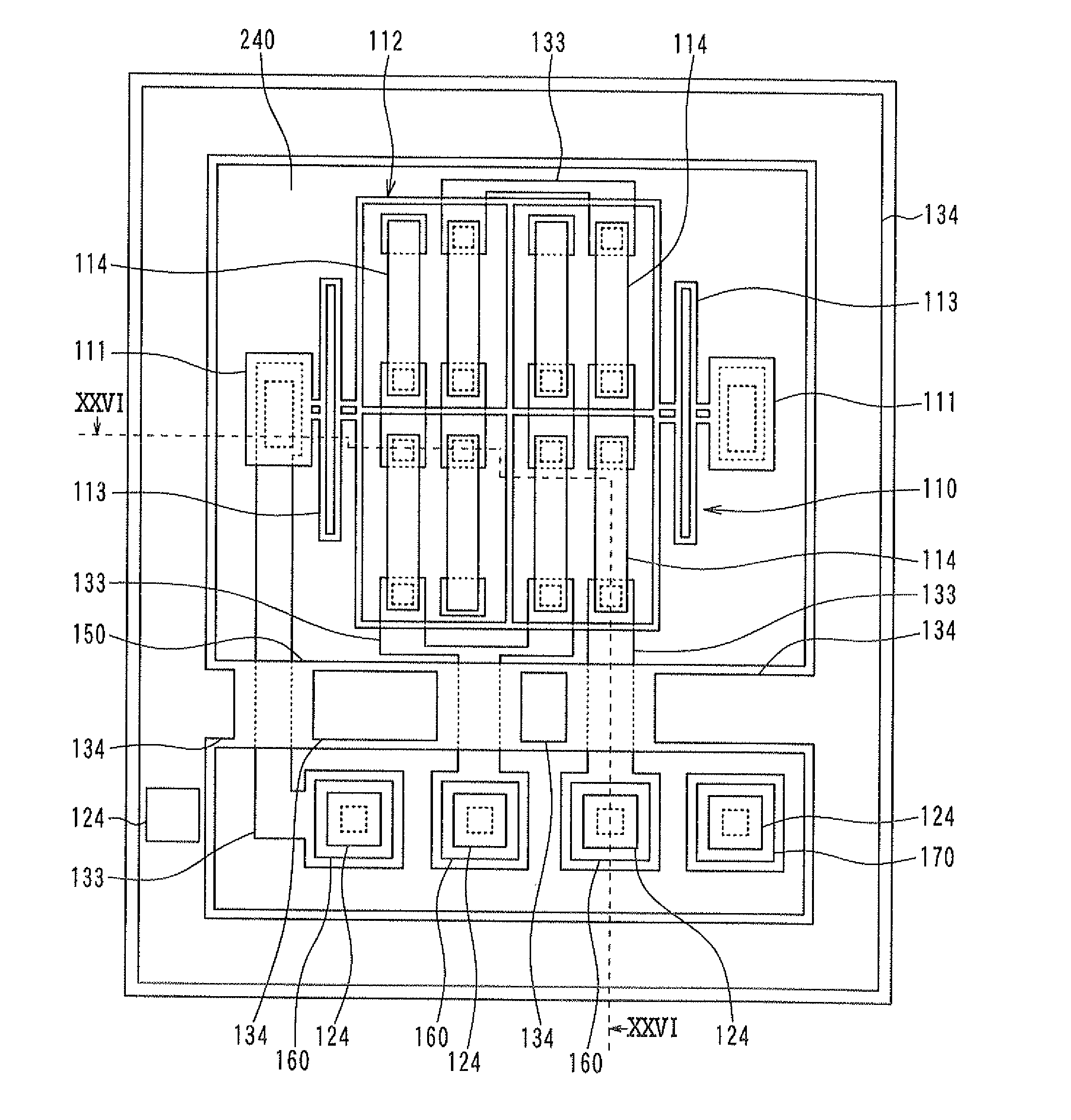
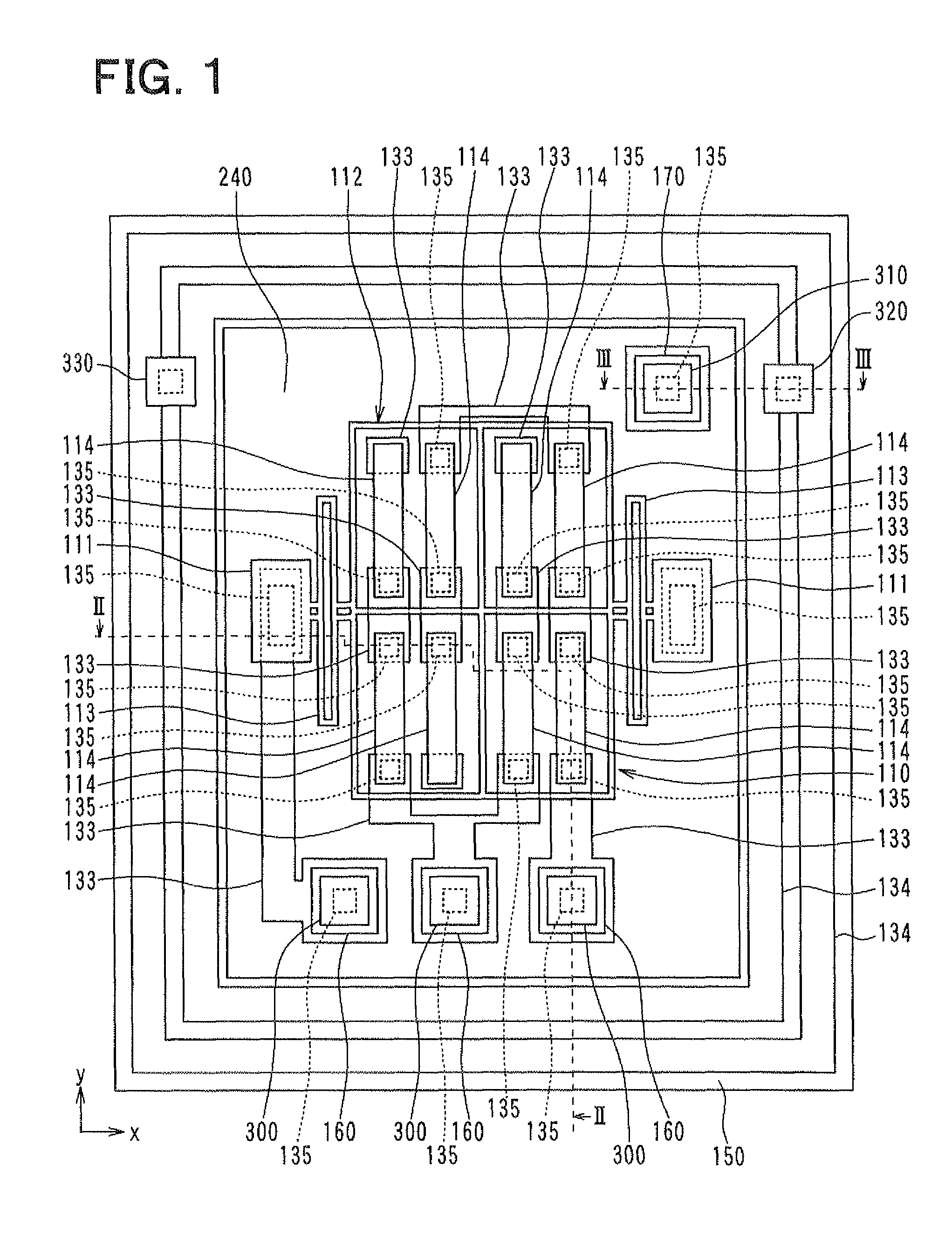
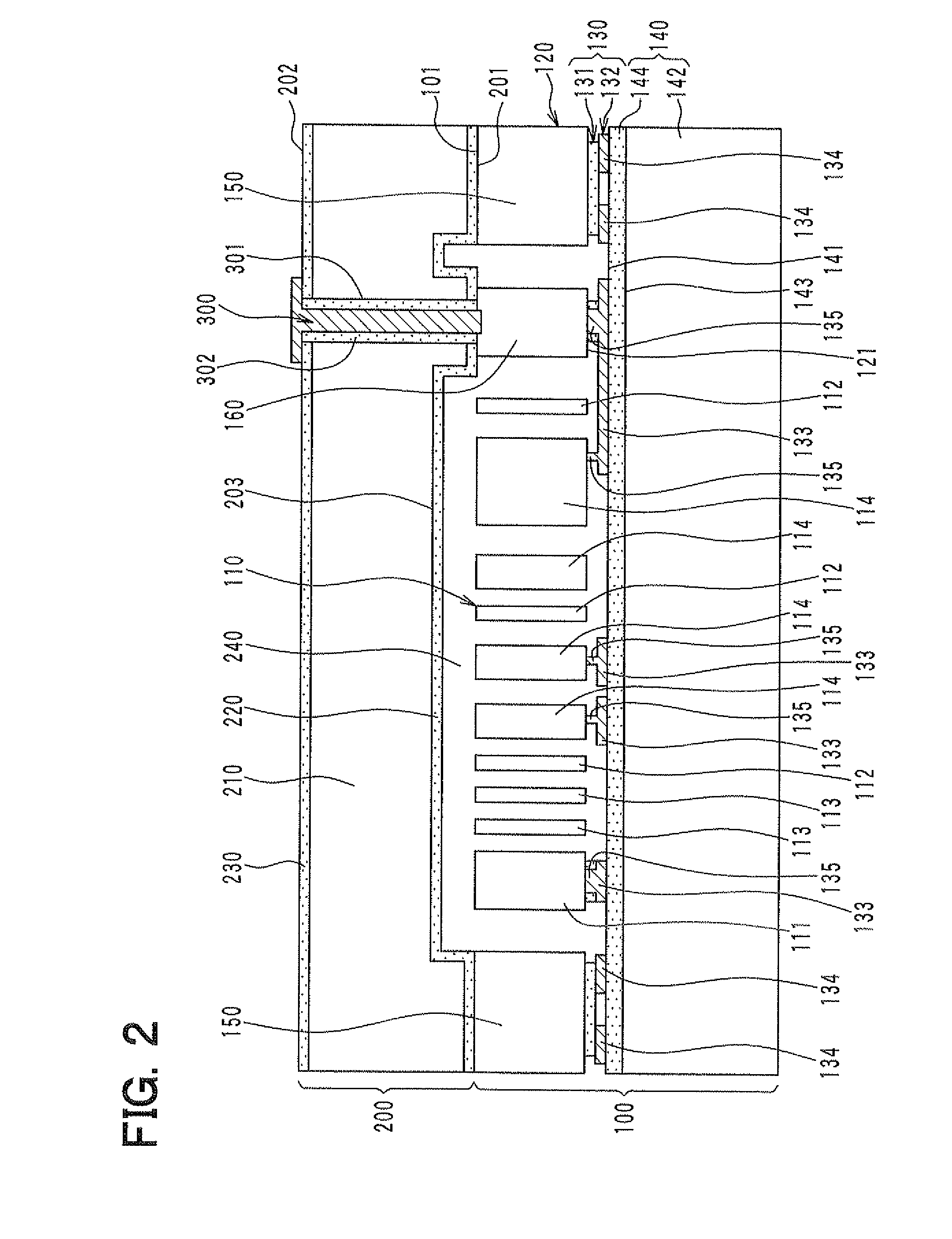
[0049]A first embodiment of the present invention will be described hereinafter with reference to the drawings. FIG. 1 is a plan view of a semiconductor physical quantity sensor according to the present embodiment. FIG. 2 is a cross-sectional view taken along a line II-II in FIG. 1. FIG. 3 is a cross-sectional view taken along a line III-III in FIG. 1. A structure of a semiconductor physical quantity sensor according to the present embodiment will be described with reference to FIGS. 1 through 3.

[0050]As shown in FIGS. 2 and 3, the semiconductor physical quantity sensor is constructed of a sensor unit 100 and a cap 200, which are bonded to each other. The sensor unit 100 has a generally plate shape including a surface 101. The cap 200 has a generally plate shape including a first surface 201 and a second surface 202 opposite to the first surface 201. The surface 101 of the sensor unit 100 and the first surface 201 of the cap 200 are bonded to each other. FIG. 1 is a plan view in whi...

second embodiment

[0127]A second embodiment will be described hereinafter with reference to FIG. 11. A structure different from the first embodiment will be mainly described. FIG. 11 is a cross-sectional view of a semiconductor physical quantity sensor according to the present embodiment, taken along a line corresponding to the II-II line in FIG. 1.

[0128]As shown in FIG. 11, the semiconductor physical quantity sensor has bonding balls 350 on the pads of the first penetrating electrodes 300, in addition to the structure of the first embodiment. The semiconductor physical quantity sensor further has the bonding balls 350 on the pads of the second and third penetrating electrodes 310, 320.

[0129]The bonding balls 350 are made of Au, solder, or the like. In this case, the semiconductor physical quantity sensor can be bonded to a circuit board by a ball-bonding technique.

third embodiment

[0130]A third embodiment will be described hereinafter with reference to FIGS. 12 through 14B. A structure different from the first and second embodiments will be mainly described. In the above-described embodiments, the first to fourth penetrating electrodes 300, 310, 320, 330 are disposed in the cap 200. In the present embodiment, on the other hand, the first penetrating electrodes 300, the second penetrating electrode 310 and the third penetrating electrode 320 are disposed in the support substrate 140.

[0131]FIG. 12 is a plan view of a semiconductor physical quantity sensor according to the present embodiment. FIG. 13 is a cross-sectional view taken along a line XIII-XIII in FIG. 12. FIG. 14A is a cross-sectional view taken along a line XIVA-XIVA in FIG. 12. FIG. 14B is a cross-sectional view taken along a line XIVB-XIVB in FIG. 12. FIG. 12 is a plan view in which the cap 200 and some parts are illustrated as transparent to show underneath structures for explanatory purposes.

[013...


PUM


Abstract

In a semiconductor physical quantity sensor, a pattern portion including a wiring pattern as a wiring is formed on a surface of a first semiconductor substrate. A support substrate having a surface made of an electrically insulating material is prepared. The first semiconductor substrate is joined to the support substrate by bonding the pattern portion to the surface of the support substrate. Further, a sensor structure is formed in the first semiconductor substrate. The sensor structure is electrically connected to the wiring pattern. A cap is bonded to the first semiconductor substrate such that the sensor structure is hermetically sealed.

Description

CROSS REFERENCE TO RELATED APPLICATION[0001]This application is based on Japanese Patent Application No. 2010-60565 filed on Mar. 17, 2010, the disclosure of which is incorporated herein by reference.FIELD OF THE INVENTION[0002]The present invention relates to a semiconductor physical quantity sensor and a method of manufacturing the same.BACKGROUND OF THE INVENTION[0003]A semiconductor physical quantity sensor constructed by joining two substrates has been proposed. For example, Japanese Patent Application Publication No. 11-267777 (counterpart U.S. Pat. No. 6,028,332) describes a semiconductor-type yaw rate sensor in which a lower wiring layer is formed on a substrate and another substrate formed with a beam structure for detecting a yaw rate is laid on the lower wiring layer.[0004]Such a yaw rate sensor is manufactured in the following manner. First, a first polycrystalline silicon layer as the lower wiring layer is formed on a first silicon substrate. Next, the first polycrystal...

Claims


Application Information

Patent Timeline
Patent Type & Authority Patents(United States)
IPC IPC(8): G11C11/15
CPCG01P15/0802B81B7/0006B81B2201/0235B81B2203/0307B81B2207/095G01P15/125G01P2015/0814G01P2015/0877G01P2015/088H01L2224/48463
Inventor FUJII, TETSUOGOTOH, KEISUKE
Owner DENSO CORP
Why Eureka
Try Eureka