Photomask and semiconductor apparatus manufacturing method

a manufacturing method and semiconductor technology, applied in the direction of photomechanical equipment, photo-taking processes, instruments, etc., can solve the problem of difficult to densely arrange the patterns

Active Publication Date: 2014-10-07
CANON KK
View PDF7 Cites 3 Cited by
  • Summary
  • Abstract
  • Description
  • Claims
  • Application Information

AI Technical Summary

Benefits of technology

[0006]The present invention provides a technique advantageous in terms of densely transferring adjacent patterns when a plurality of regions on a substrate are exposed individually.

Problems solved by technology

However, in the method disclosed in Japanese Patent Laid-Open No. 1-276717, it is necessary to ensure a large interval between adjacent patterns according to the increase in width of the pattern, thus making it difficult to densely arrange these patterns.

Method used


Image

  • Photomask and semiconductor apparatus manufacturing method
  • Photomask and semiconductor apparatus manufacturing method
  • Photomask and semiconductor apparatus manufacturing method

Examples


first embodiment

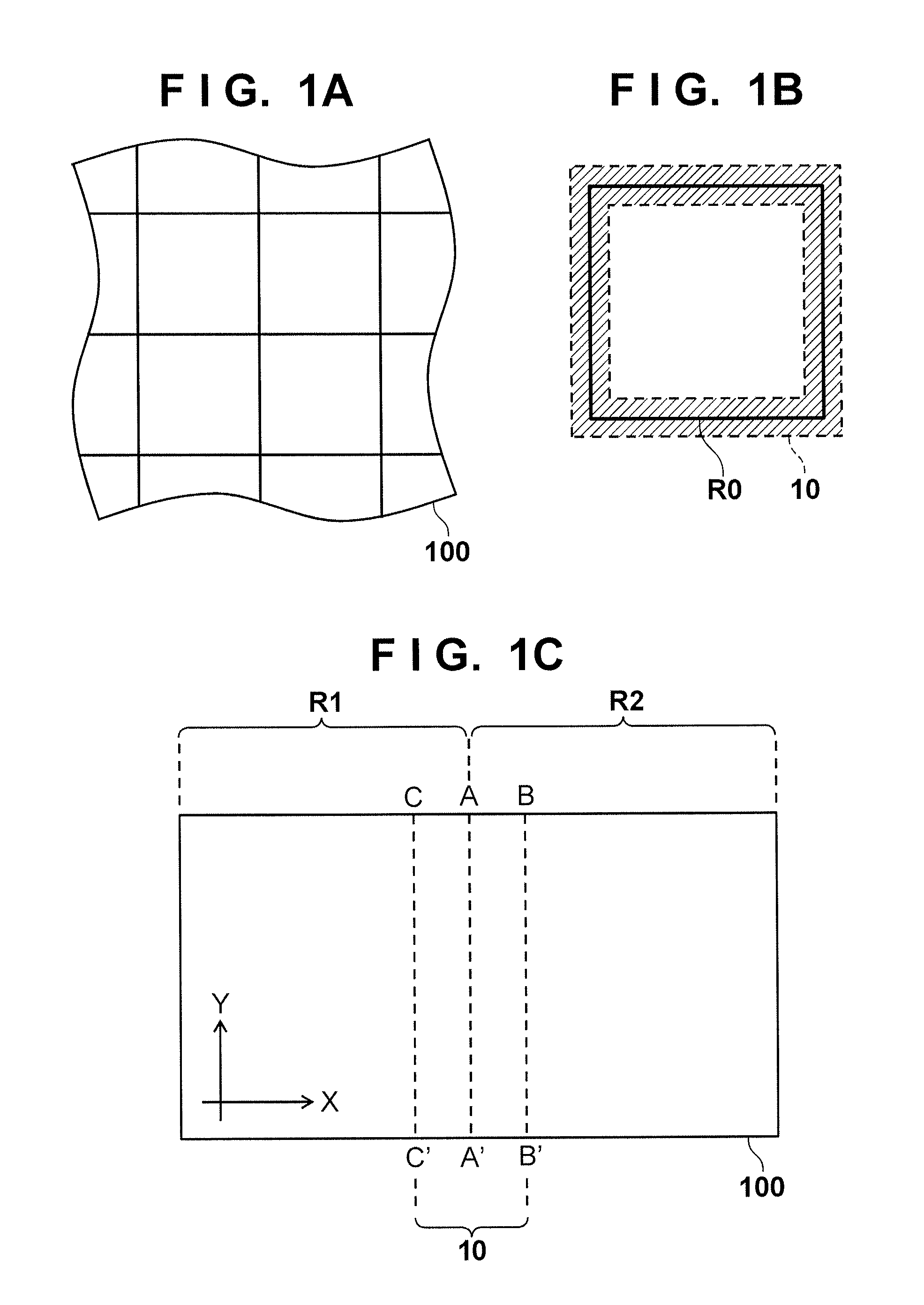
[0014]A photomask and a semiconductor apparatus manufacturing method (especially an exposure method) according to the first embodiment will be described with reference to FIGS. 1A to 3B. As illustrated in FIG. 1A, when a region in which a device or chip is to be formed on a substrate 100 is divided into a plurality of regions, and the plurality of regions are exposed individually, a portion (to be referred to as a “peripheral portion” hereinafter) which reflects an alignment error of a photomask is formed on the periphery of each region. FIG. 1B shows one region R0 of the plurality of regions, and its peripheral portion 10. The peripheral portion 10 includes inner and outer parts of the region R0. That is, the mask pattern of each photomask used in a corresponding exposure process includes the pattern of a region in which a device or chip is to be formed, and the pattern of the peripheral portion of the region. Line patterns to extend across the region R0 and adjacent regions, for e...

second embodiment

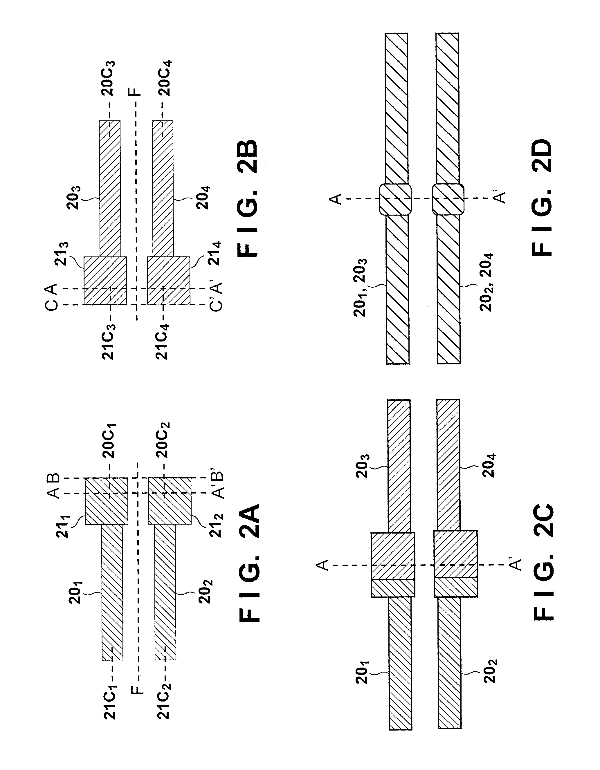
[0022]A photomask and a semiconductor apparatus manufacturing method (especially an exposure method) according to the second embodiment will be described with reference to FIGS. 4A to 4D. As in the first embodiment, the case wherein a semiconductor integrated circuit pattern is formed by individually exposing two adjacent regions (a first region R1 and a second region R2) on a substrate will be considered below.

[0023]First, a first region R1 and its peripheral portion 10 on a substrate 100 coated with, for example, a positive photoresist material are exposed using a photomask for forming a pattern as illustrated in FIG. 4A (first step). The mask pattern of the photomask used in the first step includes first to third line patterns 401 to 403 and first to third connection patterns 411 to 413. Each of the first line pattern 401 and second line pattern 402 is arranged in the first region R1 along a first direction X. The third line pattern 403 is arranged in the first region R1 along th...

third embodiment

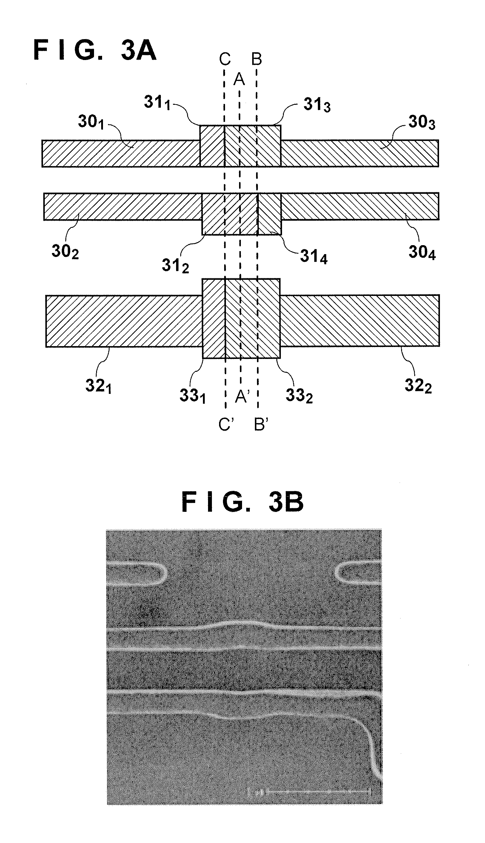
[0028]The third embodiment will be described with reference to FIGS. 5A to 5D. The third embodiment is different from the second embodiment in the following points. First, the distance from a virtual line F1 to a center line 41C1 of a first connection pattern 411 is larger than that from the virtual line F1 to a center line 40C1 of a first line pattern 401, as shown in FIG. 5A. Note that the virtual line F1 runs in a first direction X between the first line pattern 401 and a third line pattern 403. Also, the distance from a virtual line F2 to a center line 41C2 of a second connection pattern 412 is larger than that from the virtual line F2 to a center line 40C2 of a second line pattern 402, as shown in FIG. 5B. Note that the virtual line F2 runs in the first direction X between the second line pattern 402 and the third line pattern 403. The virtual line F1 and the Virtual line F2 extend along the first direction X.

[0029]For example, the first to third connection patterns 411 to 413 ...


PUM

PropertyMeasurementUnit
wavelengthaaaaaaaaaa
distancesaaaaaaaaaa
widthaaaaaaaaaa

Abstract

A photomask for exposing a region on a substrate, with a mask pattern, including a first line pattern, a second line pattern, a first connection pattern for a peripheral portion of the region and a second connection pattern for the peripheral portion, wherein the first connection pattern is wider than the first line pattern and the second connection pattern is wider than the second line pattern, a distance from a virtual line between the first line pattern and the second line pattern to a center line of the first connection pattern is larger than a distance from the virtual line to a center line of the first line pattern and a distance from the virtual line to a center line of the second connection pattern is larger than a distance from the virtual line to a center line of the second line pattern.

Description

BACKGROUND OF THE INVENTION[0001]1. Field of the Invention[0002]The present invention relates to a photomask and a semiconductor apparatus manufacturing method.[0003]2. Description of the Related Art[0004]As a method of forming, on a substrate, a device or chip with a size larger than that of the maximum shot region of an exposure apparatus, there is a method for dividing a region in which a device or chip is to be formed into a plurality of regions, and individually exposing the plurality of regions. In such a case, a pattern which reflects an alignment error of a photomask can be formed on the boundary portion between these regions. Japanese Patent Laid-Open No. 1-276717, for example, discloses a method of increasing the width of a pattern for one of two adjacent regions of the plurality of regions, and transferring a pattern with a larger length to the other region.[0005]However, in the method disclosed in Japanese Patent Laid-Open No. 1-276717, it is necessary to ensure a large ...

Claims


Application Information

Patent Timeline
Patent Type & Authority Patents(United States)
IPC IPC(8): G03F1/50G03F7/20G03F1/00
CPCG03F1/00G03F7/20G03F7/2022G03F1/50
Inventor HIRAYAMA, SATOSHIKANOME, ATSUSHI
Owner CANON KK
Why Eureka
Try Eureka