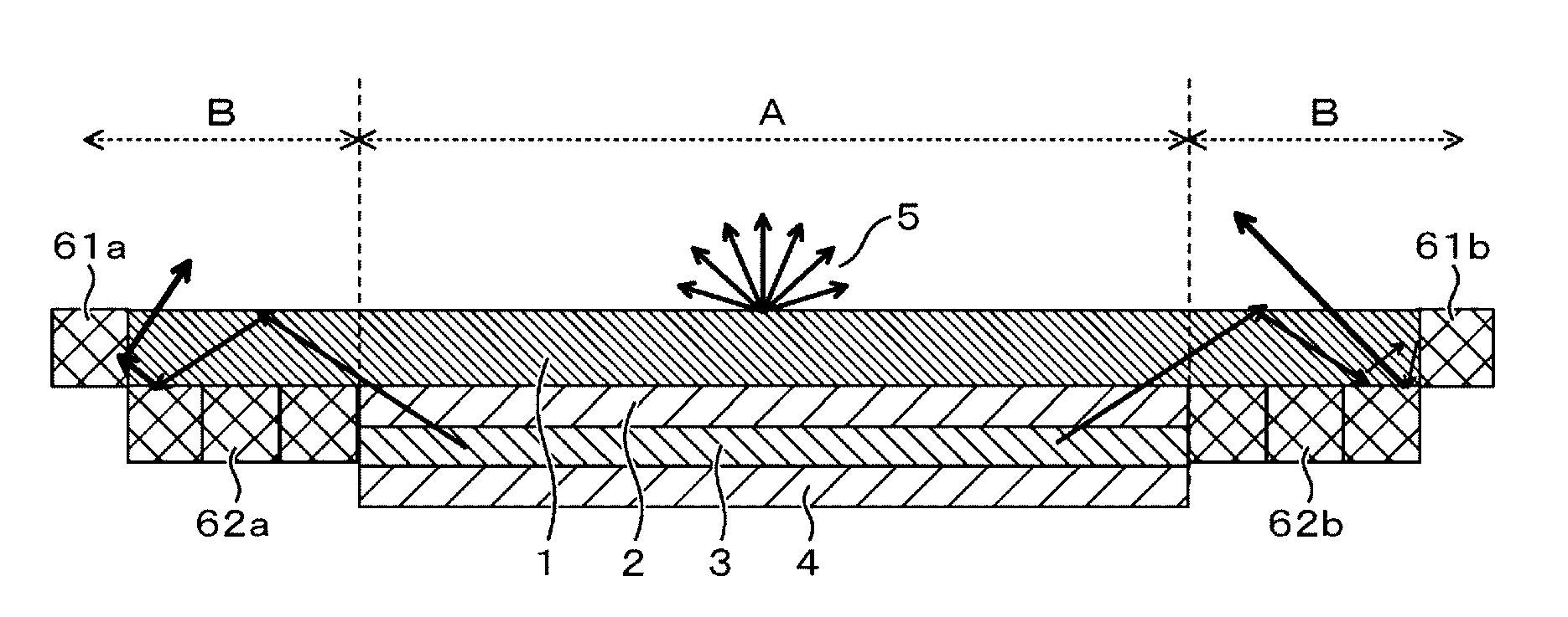
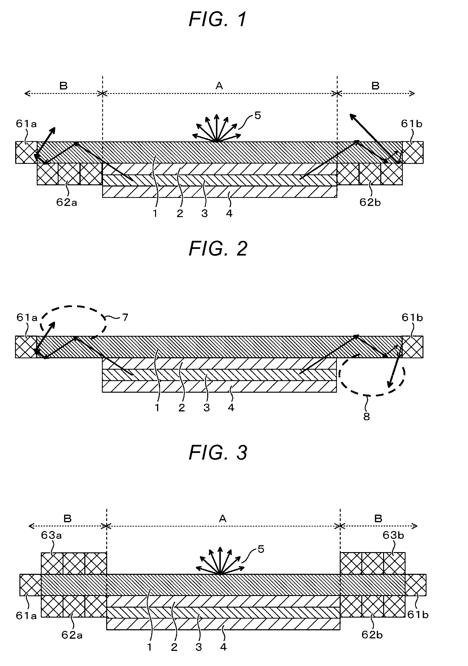
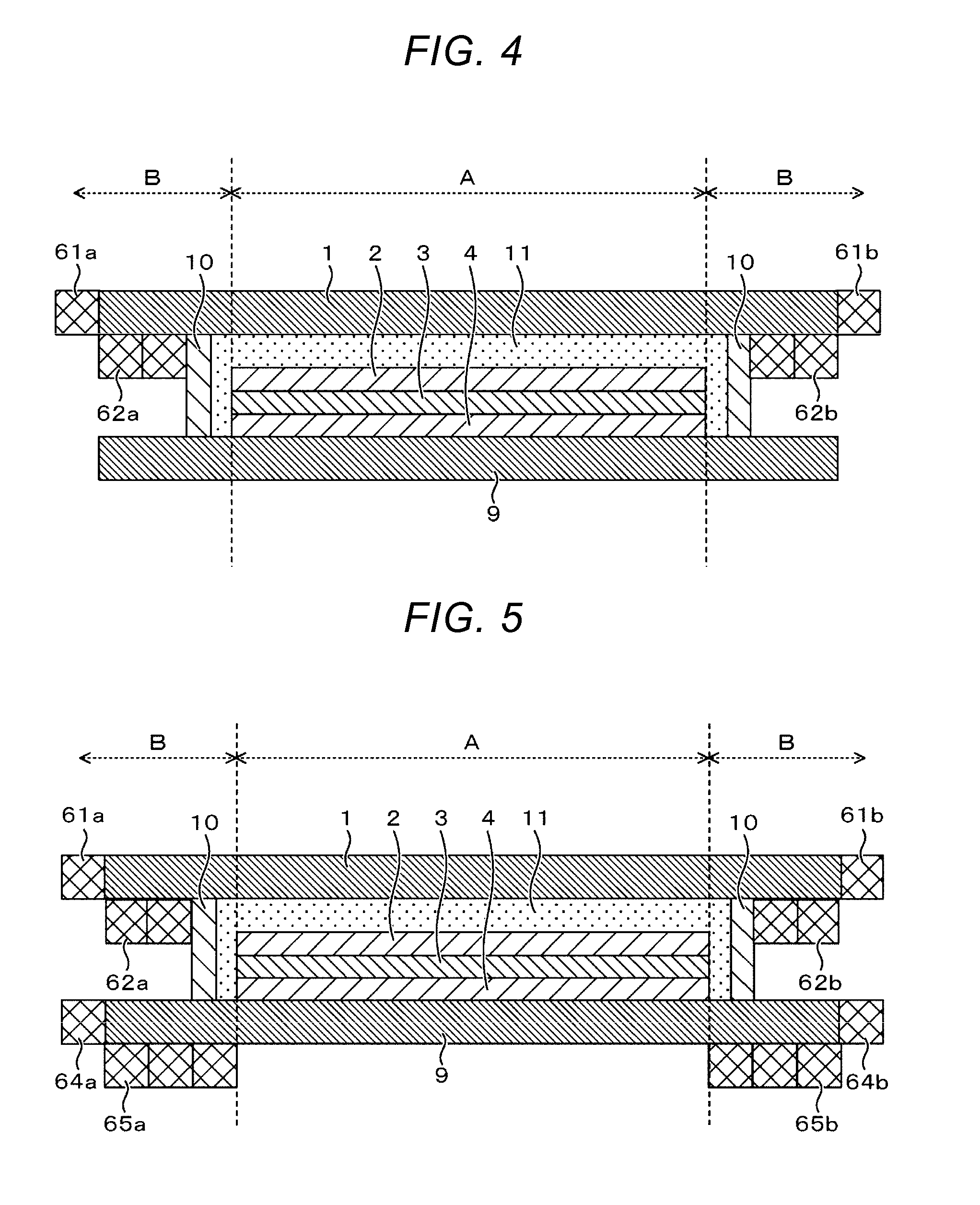
[0019]As the front substrate 1, a transparent glass plate made of soda-lime glass, alkali-free glass, or the like, or a transparent plastic plate made of an acrylic resin, a PET resin, a PEN resin, a cycloolefin resin, an olefin resin, a carbonate resin, a nylon resin, a fluorine resin, a silicone resin, a polyimide resin, a polysulfone resin, or the like can be used. The front substrate 1 may be any as long as it has light transmissibility, and a slightly colored one may be used other than a colorless transparent one. In particular, one which transmits light with a wavelength of from 380 to 780 nm is preferred. Further, the refractive index of the front substrate 1 is not particularly limited, but is preferably 1.6 or more. By using the front substrate 1 having a refractive index of 1.6 or more, the total reflection occurring at the interface between the transparent electrode 2 and the front substrate 1 at which the refractive index changes can be prevented, and light which is guided in the transparent electrode 2 and lost can be extracted to the front substrate 1, and therefore, the effect of the invention that light trapped in the substrate is extracted to air can be further improved. As the front substrate 1 having a high refractive index, for example, a high-refractive index glass containing antimony, zinc, zirconium, tantalum, tungsten, lead, or the like, a plastic having a refractive index increased by the introduction of chlorine, bromine, iodine, sulfur, or the like, a plastic having a refractive index increased by crystallization through stretching, or the like can be used. Specific examples of a commercially available product include a variety of optical glasses manufactured by Sumita Optical Glass, Inc.
[0020]The transparent electrode 2 formed as an anode is an electrode for injecting holes into the organic light-emitting layer 3. As the transparent electrode 2 (anode), an electrode material composed of a metal, an alloy, an electroconductive compound, or a mixture thereof, each having a high work function is preferably used, and particularly, an electrode material having a work function of 4 eV or more is preferably used. Specific examples of such an electrode material include metals such as gold and conductive transparent materials such as CuI, ITO (indium tin oxide), SnO2, ZnO, and IZO (indium zinc oxide). For example, by depositing such an electrode material on the front substrate 1 using a vacuum deposition method, a sputtering method, a CVD method, an ion plating method, a coating method, or the like, the transparent electrode 2 (anode) in the form of a thin film can be formed. The light transmittance of the transparent electrode 2 (anode) is preferably 80% or more. Further, the sheet resistance of the transparent electrode 2 (anode) is preferably several hundreds Ω / sq. or less, particularly preferably 100 Ω / sq. or less. Further, in order to control the properties of the transparent electrode 2 (anode) such as transparency and conductivity as described above, the film thickness of the transparent electrode 2 (anode) is set to 80 to 400 nm, more preferably 100 to 200 nm, although it varies depending on the material thereof.Organic Light-Emitting Layer
[0021]The organic light-emitting layer 3 is composed of a hole transport layer, a light-emitting layer, an electron transport layer, a buffer layer, and the like. However, the organic light-emitting layer may not have a hole transport layer, an electron transport layer, or a buffer layer as long as it has at least a light-emitting layer. Further, the organic light-emitting layer may have a hole injection layer or an electron injection layer, which will be described later, in some cases.
[0022]The hole transport layer has a function of transporting holes and injecting the holes into the light-emitting layer. Therefore, the hole transport layer is preferably composed of a hole transport material having a high hole mobility. Further, it is preferred that the hole transport layer is chemically stable and has a low ionization potential, a low electron affinity, and a high glass transition temperature. As a material of the hole transport layer, for example, N,N′-bis(3-methylphenyl)-N,N′-diphenyl-[1,1′-biphenyl]-4,4′-diamine (TPD), 4,4′-bis[N-(1-naphthyl)-N-phenylamino]biphenyl (α-NPD), 4,4′,4″-tri(N-carbazolyl)triphenylamine (TCTA), 1,3,5-tris[N-(4-diphenylaminophenyl)phenylamino]benzene (p-DPA-TDAB), 4,4′,4″-tris(N-carbazol)triphenylamine (TCTA), 1,3,5-tris[N,N-bis(2-methylphenyl)-amino]-benzene (o-MTDAB), 1,3,5-tris[N,N-bis(3-methylphenyl)-amino]-benzene (m-MTDAB), 1,3,5-tris[N,N-bis(4-methylphenyl)-amino]-benzene (p-MTDAB), 4,4′,4″-tris[1-naphthyl(phenyl)amino]triphenylamine (1-TNATA), 4,4′,4″-tris[2-naphthyl(phenyl)amino]triphenylamine (2-TNATA), 4,4′,4″-tris[biphenyl-4-yl-(3-methylphenyl)amino]triphenylamine (p-PMTDATA), 4,4′,4″-tris[9,9-dimethylfluorene-2-yl(phenyl)amino]triphenylamine (TFATA), 4,4′,4″-tris(N-carbazoyl)triphenylamine (TCTA), 1,3,5-tris[N-(4-diphenylaminophenyl)phenylamino]benzene (p-DPA-TDAB), 1,3,5-tris{4-[methylphenyl(phenyl)amino]phenyl}benzene (MTDAPB), N,N′-di(biphenyl-4-yl)-N,N′-diphenyl[1,1′-biphenyl]-4,4′-diamine (p-BPD), N,N′-bis(9,9-dimethylfluorene-2-yl)-N,N′-diphenylfluorene-2,7-diamine (PFFA), N,N,N′,N′-tetrakis(9,9-dimethylfluoren-2-yl)-[1,1-biphenyl]-4,4′-diamine (FFD), (NDA)PP, 4-4′-bis[N,N′-(3-tollyl)amino]-3-3′-dimethylbiphenyl (HMTPD), etc. are preferred, and these may be used alone or in combination of two or more of them.
[0023]A hole injection layer may be disposed between the transparent electrode 2 serving as an anode and the hole transport layer as needed. The hole injection layer is preferably formed from a material having an appropriate ionization potential so as to reduce a hole injection barrier between the anode and the hole transport layer. Further, it is preferred that the hole injection layer plays a role in burying the unevenness of a surface of an under layer. Examples of the material of the hole injection layer include copper phthalocyanine, a star burst amine compound, polyaniline, polythiophene, vanadium oxide, molybdenum oxide, ruthenium oxide, and aluminum oxide.
[0024]The hole transport material may contain an oxidant. By incorporating an oxidant in the hole transport material, the barrier between the anode and the hole transport layer can be reduced, or the electroconductivity can be improved. Examples of the oxidant include Lewis acid compounds such as ferric chloride, ammonium chloride, gallium chloride, indium chloride, and antimony pentachloride, electron accepting compounds such as trinitrofluorene, and compounds listed as the material of the hole injection layer such as vanadium oxide, molybdenum oxide, ruthenium oxide, and aluminum oxide, and these may be used alone or in combination of two or more of them.


