Semiconductor device and manufacturing method thereof

a semiconductor device and manufacturing method technology, applied in the direction of semiconductor devices, electrical appliances, transistors, etc., can solve the problems of low voltage at which the transistor is turned on, low power consumption, and degradation of the characteristics of the transistor, so as to reduce the power consumption of the semiconductor device, increase the number of steps, and improve the quality of the semiconductor film

Active Publication Date: 2012-06-21
SEMICON ENERGY LAB CO LTD
View PDF49 Cites 20 Cited by
  • Summary
  • Abstract
  • Description
  • Claims
  • Application Information

AI Technical Summary

Benefits of technology

[0012]An object is to manufacture a transistor whose threshold voltage is controlled without using a backgate electrode, a circuit for controlling the threshold voltage, and an impurity introduction method. An object is to manufacture a semiconductor device having favorable electrical characteristics, high reliability, and low power consumption using the transistor. Further, an object is to form a gate electrode material applicable to the transistor.
[0014]The work function of the tungsten oxide film can be controlled by adjustment of the composition of the tungsten oxide film. By using the tungsten oxide film whose work function is controlled as part of the gate electrode, the threshold voltage of the transistor can be controlled.
[0019]In order to control the work function, a material containing one or more elements selected from Mg, Al, Ti, V, Cr, Mn, Co, Ni, Cu, Zn, Ga, Y, Zr, Nb, Mo, Ag, In, Sn, La, Ce, Nd, Hf, and Ta may be mixed in the target. For example, molybdenum oxide which is an oxide of Mo is known to have a high work function. However, molybdenum oxide is highly reactive with plasma and a chemical solution and soluble in water; thus it is hard to use molybdenum oxide as a single film. In contrast, a mixture of tungsten oxide and molybdenum oxide has lower reactivity with plasma and a chemical solution, is relatively stable, and is suitable for the control of the work function. Therefore, the mixture of tungsten oxide and molybdenum oxide is preferable due to less limitations on the process.
[0025]In the above-described manner, with an embodiment of the present invention, a transistor whose threshold voltage is controlled without using a backgate electrode, a circuit for controlling the threshold voltage, and an impurity introduction method can be manufactured. The control of the threshold voltage of the transistor enables a reduction in the power consumption of a semiconductor device that uses an embodiment of the present invention.
[0026]An embodiment of the present invention is made by devising the gate electrode and does not increase the number of steps for manufacturing a transistor. In addition, degradation of the quality of a semiconductor film due to the impurity introduction is not caused. Therefore, a semiconductor device having favorable electrical characteristics and high reliability can be manufactured with high productivity.
[0027]A semiconductor device having favorable electrical characteristics, high reliability, and low power consumption can be manufactured with high productivity.

Problems solved by technology

For example, when the threshold voltage is close to 0 V in a transistor, the voltage at which the transistor is turned on can be low, leading to low power consumption.
For example, in the case of using a silicon-based semiconductor material for an active layer, the threshold voltage can be controlled by introducing a Group 13 element or a Group 15 element into the active layer; however, it is known that the introduction of a Group 13 element or a Group 15 element reduces the crystallinity and causes impurity scattering and the like, leading to degradation of transistor characteristics.
This technique shifts the threshold voltage to the positive side but has problems of low resistance of the molybdenum oxide to a later plasma process and recession of the molybdenum oxide layer.

Method used


Image

  • Semiconductor device and manufacturing method thereof
  • Semiconductor device and manufacturing method thereof
  • Semiconductor device and manufacturing method thereof

Examples


embodiment 1

[0053]A method of forming a tungsten oxide film whose composition is adjusted, which is an embodiment of the present invention, will be described.

[0054]In the case of forming a tungsten oxide film by a sputtering method, a tungsten oxide target, a tungsten nitride target, or a tungsten target is used. By adjusting the composition of the target, the composition of the film can be controlled.

[0055]For example, the composition of the target can be adjusted by changing the mixing ratio of tungsten, tungsten dioxide, or tungsten trioxide (or tungsten oxide with another valence) in manufacturing the target, whereby the composition of the film to be obtained can be adjusted. Variation in the mixing ratio of materials can produce a variety of work functions; in this manner, the work function can be controlled.

[0056]The composition of the film can also be adjusted by mixing tungsten nitride in a tungsten oxide target.

[0057]In order to control the work function, a material containing one or m...

embodiment 2

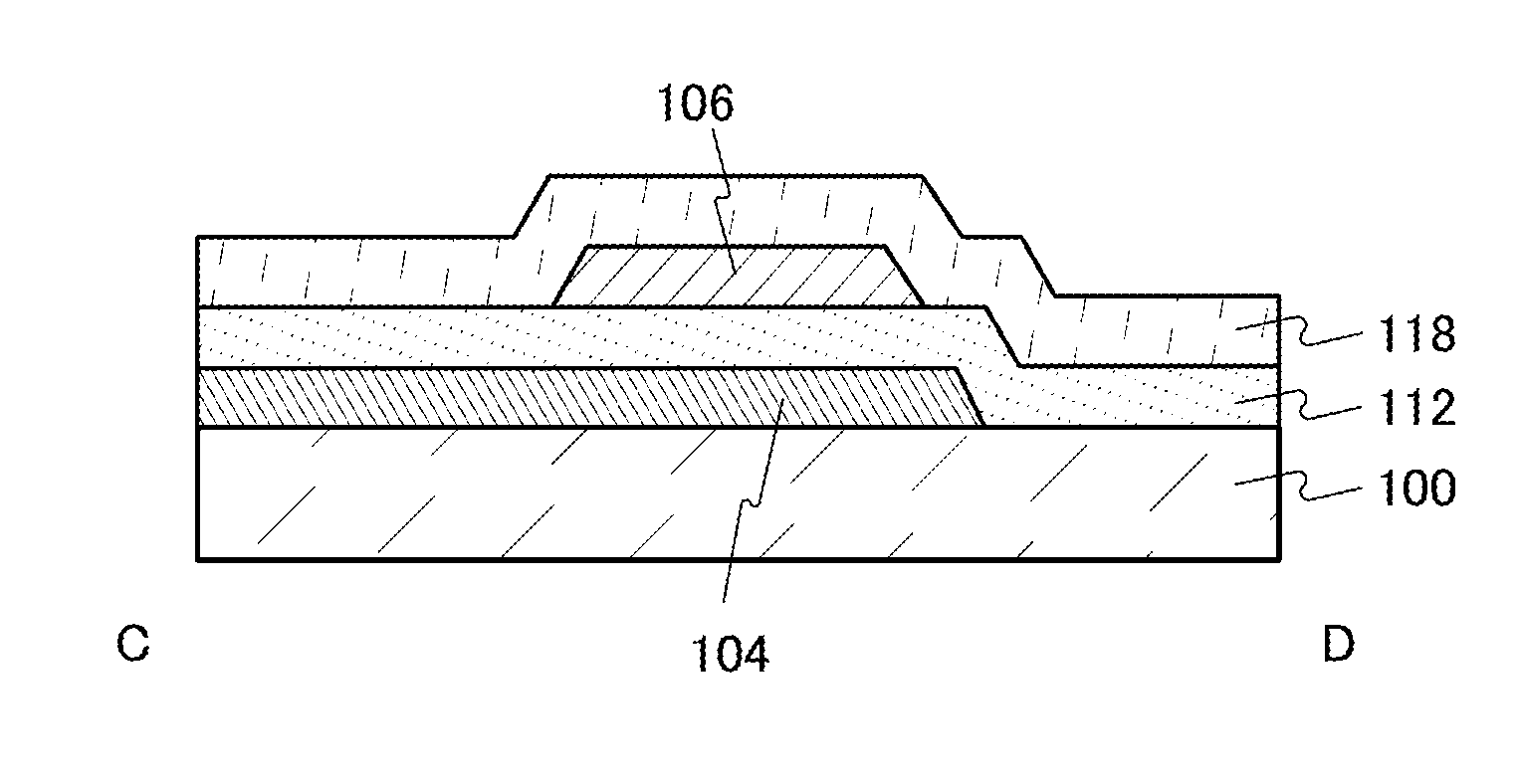
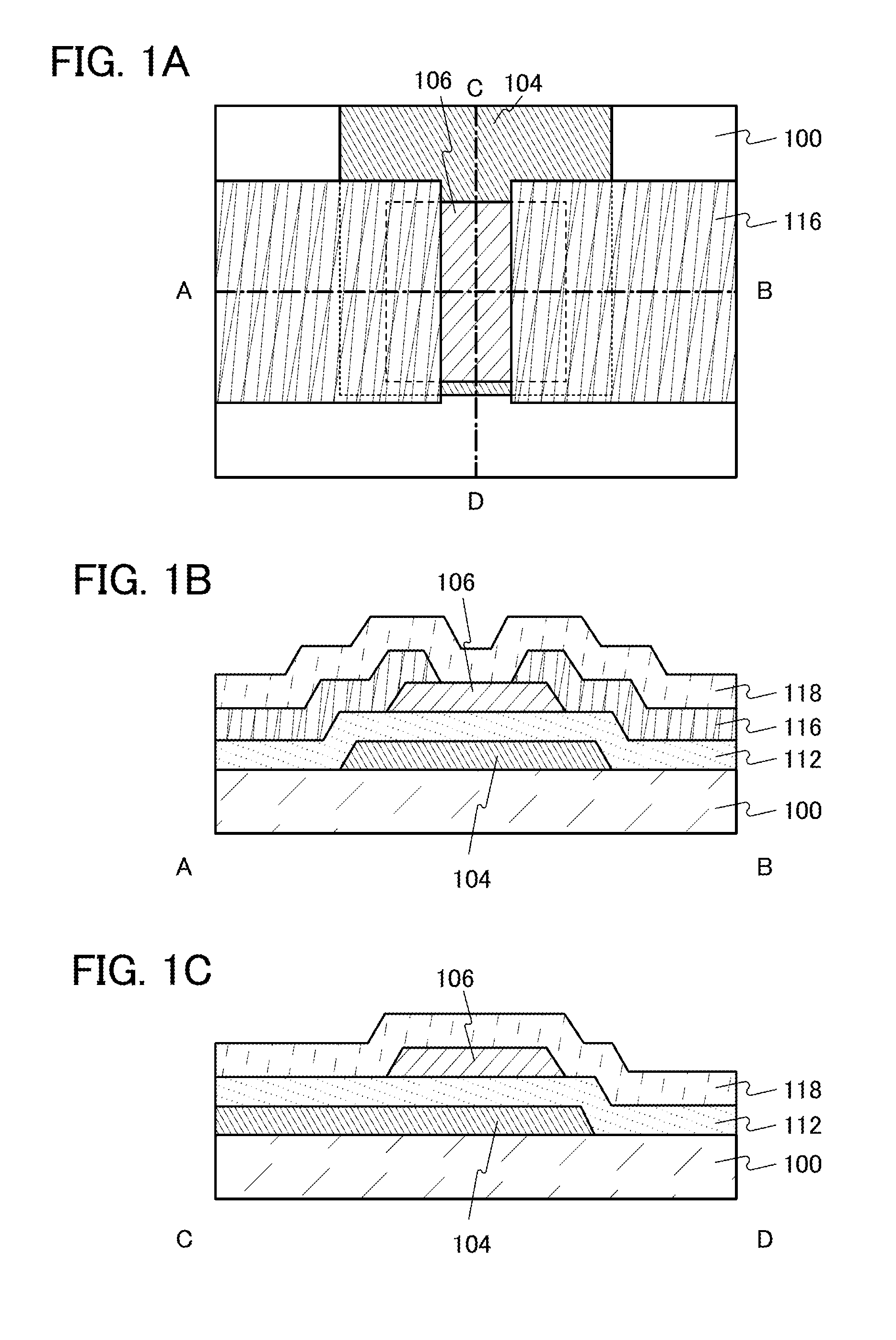
[0072]A transistor which is an embodiment of the present invention will be described with reference to FIGS. 1A to 1C.

[0073]FIGS. 1A to 1C are a top view and cross-sectional views of a transistor which is an embodiment of the present invention. A cross section A-B in FIG. 1B and a cross section C-D in FIG. 1C correspond to alternate long and short dash lines A-B and C-D in FIG. 1A, respectively.

[0074]Here, the cross section A-B in FIG. 1B will be described in detail.

[0075]The cross-section A-B is a cross section of a transistor including a substrate 100, a gate electrode 104 over the substrate 100, a gate insulating film 112 that covers the substrate 100 and the gate electrode 104, a semiconductor film 106 positioned over the gate electrode 104 with the gate insulating film 112 interposed therebetween, a pair of electrodes 116 having a part in contact with the semiconductor film 106 and being over the semiconductor film 106, and an interlayer insulating film 118 that covers the gate...

embodiment 3

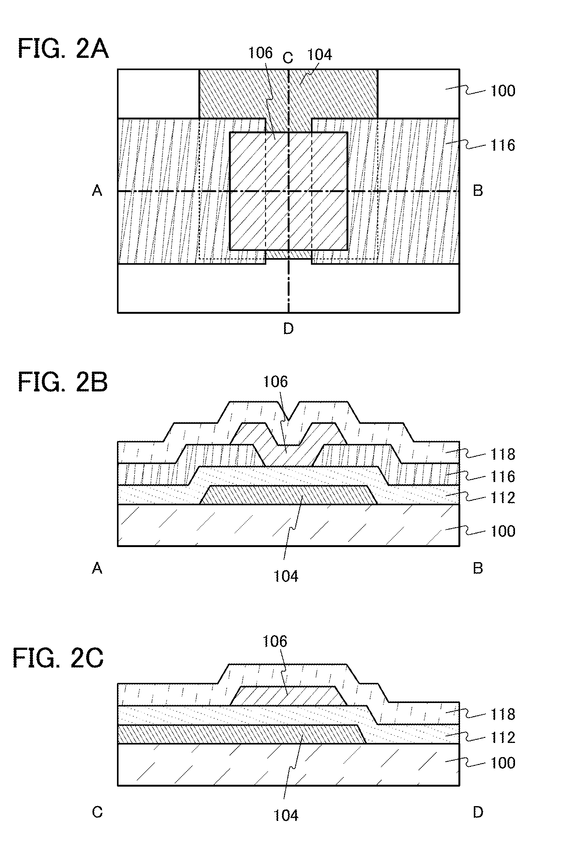
[0102]In this embodiment, a transistor having a structure different from that of the transistor described in Embodiments 2 will be described.

[0103]FIGS. 2A to 2C are a top view and cross-sectional views of a transistor which is an embodiment of the present invention. A cross section A-B in FIG. 2B and a cross section C-D in FIG. 2C correspond to alternate long and short dash lines A-B and C-D in FIG. 2A, respectively.

[0104]The cross section A-B in FIG. 2B will be described in detail below.

[0105]The cross-section A-B is a cross section of a transistor including a substrate 100, a gate electrode 104 over the substrate 100, a gate insulating film 112 that covers the substrate 100 and the gate electrode 104, a pair of electrodes 116 over the gate insulating film 112, a semiconductor film 106 having a part in contact with the pair of electrodes 116 and being over the pair of electrodes 116, and an interlayer insulating film 118 that covers the gate insulating film 112, the pair of electr...


PUM


Abstract

To manufacture a transistor whose threshold voltage is controlled without using a backgate electrode, a circuit for controlling the threshold voltage, and an impurity introduction method. To manufacture a semiconductor device having favorable electrical characteristics, high reliability, and low power consumption using the transistor. A gate electrode including a tungsten oxide film whose composition is controlled is used. The composition or the like is adjusted by a film formation method of the tungsten oxide film, whereby the work function can be controlled. By using the tungsten oxide film whose work function is controlled as part of the gate electrode, the threshold of the transistor can be controlled. Using the transistor whose threshold voltage is controlled, a semiconductor device having favorable electrical characteristics, high reliability, and low power consumption can be manufactured.

Description

BACKGROUND OF THE INVENTION[0001]1. Field of the Invention[0002]The present invention relates to a semiconductor device and a manufacturing method of the semiconductor device.[0003]In this specification, a semiconductor device means any device that can function by utilizing semiconductor characteristics; a semiconductor display device, a semiconductor circuit, an electronic device are all included in the category of the semiconductor device. 2. Description of the Related Art[0004]A technique by which transistors are formed using a semiconductor thin film formed over a substrate having an insulating surface has been attracting attention. Such transistors are applied to a wide range of electronic devices such as an integrated circuit (IC) or an image display device (display device). As materials of semiconductor thin films applicable to the transistors, there are silicon-based semiconductor materials and oxide semiconductor materials.[0005]For example, amorphous silicon, microcrystall...

Claims


Application Information

Patent Timeline
Patent Type & Authority Applications(United States)
IPC IPC(8): H01L29/786H01L21/336
CPCH01L27/1225H01L29/7869H01L29/4908H01L21/2855H01L21/28088H01L21/288H01L29/42384H01L29/66742
Inventor ENDO, YUTASASAKI, TOSHINARINODA, KOSEISATO, HITOMISATO, YUHEI
Owner SEMICON ENERGY LAB CO LTD
Why Eureka
Try Eureka