Organic light-emitting diode and method of manufacturing the same

a light-emitting diode and organic technology, applied in the direction of luminescent compositions, thermoelectric devices, chemistry apparatus and processes, etc., can solve the problems of deterioration of important diode properties such as light emission efficiency and the like, difficulty in injecting electrons from the cathode to the organic material layer, etc., and achieve high work function

Active Publication Date: 2011-07-28
LG DISPLAY CO LTD
View PDF34 Cites 21 Cited by
  • Summary
  • Abstract
  • Description
  • Claims
  • Application Information

AI Technical Summary

Benefits of technology

[0010]According to the present invention, a cathode in the organic light emitting diode of the inverted structure may be formed of a transparent electrode that is made of a material having a high work function such as a transparent metal oxide. Therefore, in the present invention, there may be provided an organic light emitting diode that is capable of emitting light in both side directions. The both-side emission organic light emitting diode is useful for the purpose of illumination.

Problems solved by technology

However, since the conductive oxide film has a very high work function, in the case of when the cathode is formed by using this, it is difficult to inject electrons from the cathode to the organic material layer.
Accordingly, operation voltage of the organic light emitting diode is largely increased, and important diode properties such as light emission efficiency and the like are deteriorated.

Method used


Image

  • Organic light-emitting diode and method of manufacturing the same
  • Organic light-emitting diode and method of manufacturing the same
  • Organic light-emitting diode and method of manufacturing the same

Examples


example 1

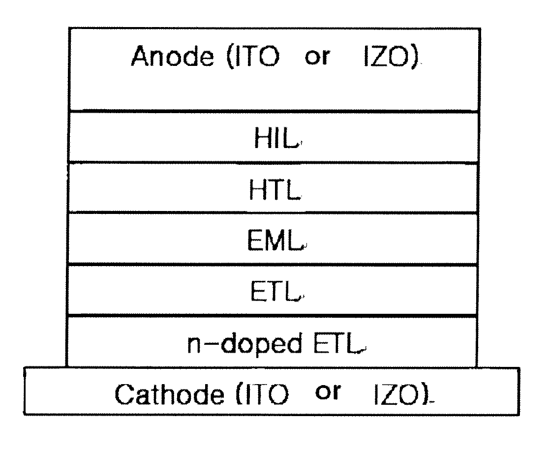
[0083]The transparent IZO cathode having the thickness of 1000 Å was formed by using the sputtering method on the substrate, and the n-type doped electron transport layer having the thickness of 50 Å was formed thereon by doping Ca on the electron transport material of the following Formula A in an amount of 10% as the first electron transport layer. Subsequently, the second electron transport layer having the thickness of 150 Å was formed on the first electron transport layer by using the electron transport material of the following Formula A.

[0084]In addition, the light emitting layer having the thickness of 300 Å was formed by depositing Alq3 (aluminium tris(8-hydroxyquinoline)) of the following Formula under the vacuum, and the hole transport layer having the thickness of 400 Å was formed thereon by depositing NPB of the following Formula under the vacuum. Subsequently, the hole injection layer having the thickness of 500 Å was formed thereon by depositing the following HAT mate...

example 2

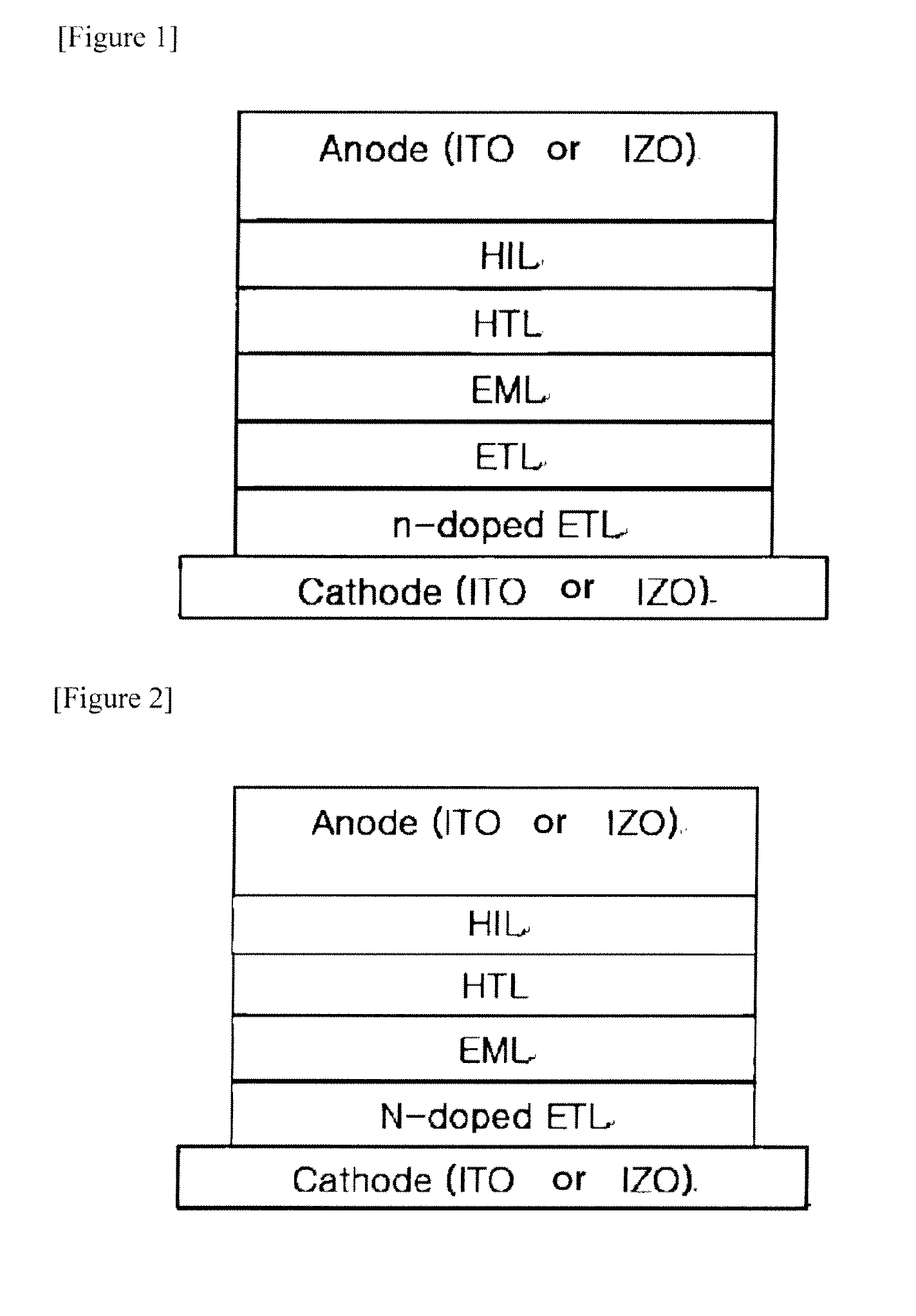
[0087]The transparent IZO cathode having the thickness of 1000 Å was formed by using the sputtering method on the substrate, and the n-type doped electron transport layer having the thickness of 200 Å was formed thereon by doping Ca on the electron transport material of the following Formula A in an amount of 10% as the electron transport layer. In addition, the light emitting layer having the thickness of 300 Å was formed by depositing Alq3 (aluminium tris(8-hydroxyquinoline)) of the Formula of Example 1 under the vacuum, and the hole transport layer having the thickness of 400 Å was formed the on by depositing NPB of the Formula under the vacuum. Subsequently, the hole injection layer having the thickness of 500 Å was formed thereon by depositing the HAT material of Example 1 under the vacuum. The IZO layer having the thickness of 1750 Å was formed thereon. In addition, the transparent IZO anode having the thickness of 1750 Å was formed on the hole injection layer.

[0088]In the abo...

example 3

[0090]The transparent IZO cathode having the thickness of 1000 Å was formed by using the sputtering method on the substrate, and the n-type electron transport layer having the thickness of 200 Å was formed thereon by doping Mg on the electron transport material of the following Formula A in an amount of 10%. The residual steps were the same as those of Example 2.

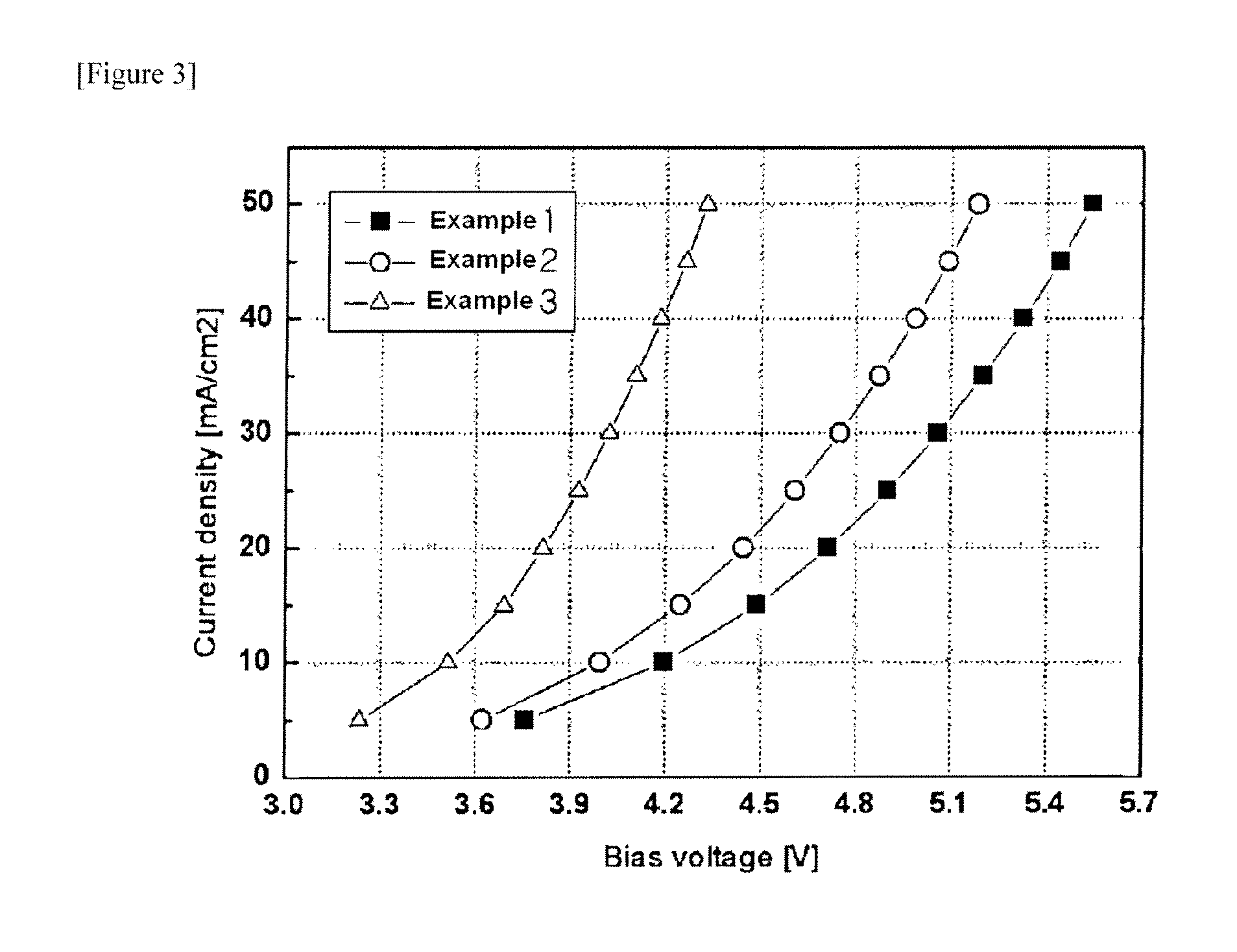
[0091]The voltage was sequentially applied to the organic light emitting diode that was manufactured in Example 3 at an interval of current density of 0.2 mA / cm2, such that each voltage and brightness leakage current were measured, and the results are shown in FIGS. 3, 4 and 5.


PUM


Abstract

The present invention provides an organic light emitting diode comprising a substrate; a transparent cathode; an anode; and an organic material layer interposed between the transparent cathode and the anode, wherein the organic material layer comprises a light emitting layer and an n-type doped electron transport layer, the n-type doped electron transport layer includes an electron transport material and an n-type dopant and is disposed between the transparent cathode and the light emitting layer, and a method for manufacturing the same.

Description

TECHNICAL FIELD[0001]The present invention relates to an organic light emitting diode and a method for manufacturing the same. More particularly, the present invention relates to an organic light emitting diode and a method for manufacturing the same, in which a transparent electrode that is made of a material having a high work function such as a transparent metal oxide is capable of being used as a cathode. This application claims priority from Korean Patent Application No. 10-2008-0096732 filed on Oct. 1, 2008 in the KIPO, the disclosure of which is incorporated herein by reference in its entirety.BACKGROUND ART[0002]An organic light emitting diode (OLED) is generally composed of two electrodes (an anode and a cathode) and one or more organic material layers that are disposed between the electrodes. In the organic light emitting diode having this structure, if a voltage is applied between the two electrodes, a hole flows from an anode and an electron flows from a cathode into an ...

Claims


Application Information

Patent Timeline
Patent Type & Authority Applications(United States)
IPC IPC(8): H01L51/54H01L33/42
CPCC09K11/06C09K2211/1007C09K2211/1011H05B33/28H01L51/0072H01L51/5052H05B33/26C09K2211/1044H10K85/6572H10K50/165H05B33/20H10K50/00
Inventor LEE, JUNG-HYOUNGSON, SE-HWANKANG, MIN-SOO
Owner LG DISPLAY CO LTD
Why Eureka
Try Eureka