Selective diffraction with in-series gratings

a selective diffraction and in-series technology, applied in the direction of optical radiation measurement, instruments, spectrometry/spectrophotometry/monochromators, etc., can solve the problems of reducing throughput, affecting the diffraction and affecting the efficiency of optical gratings

Active Publication Date: 2014-10-28
KLA CORP
View PDF13 Cites 12 Cited by
  • Summary
  • Abstract
  • Description
  • Claims
  • Application Information

AI Technical Summary

Problems solved by technology

However, as the dimensions of semiconductor devices decrease, inspection and metrology become even more important to the successful manufacture of acceptable semiconductor devices because smaller defects and deviations can cause the devices to fail.
The diffraction efficiency of an optical grating typically falls off to less than 10% when being operated relatively far away from its peak efficiency, which means that more than 90% of the available photons within a given system may be lost in that wavelength range.
A disadvantage of such a switching design is that throughput is reduced since the full spectrum measurements can only be acquired by making successive measurements.

Method used


Image

  • Selective diffraction with in-series gratings
  • Selective diffraction with in-series gratings
  • Selective diffraction with in-series gratings

Examples


Embodiment Construction

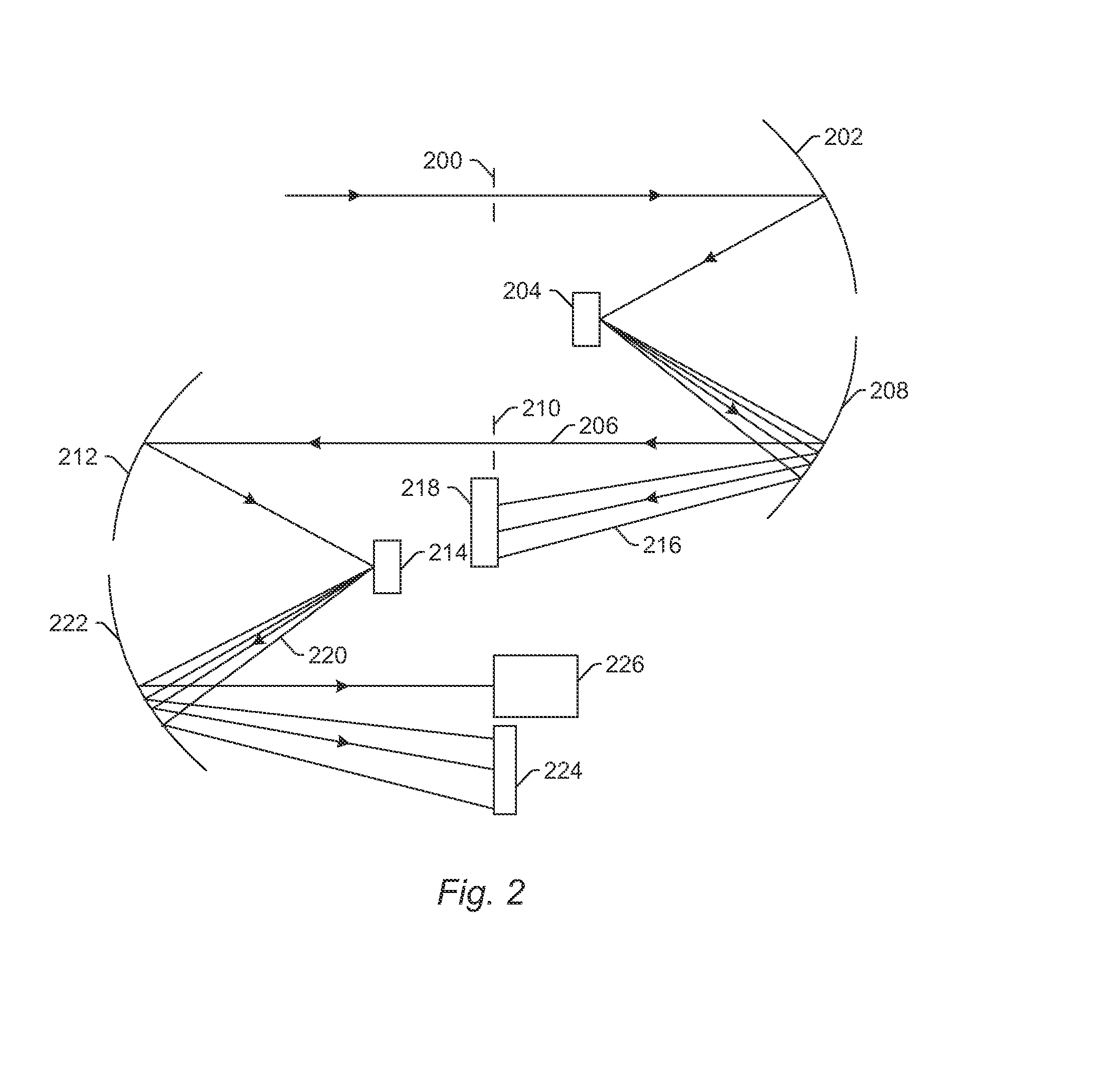
[0019]Turning now to the drawings, it is noted that the figures are not drawn to scale. In particular, the scale of some of the elements of the figures is greatly exaggerated to emphasize characteristics of the elements. It is also noted that the figures are not drawn to the same scale. Elements shown in more than one figure that may be similarly configured have been indicated using the same reference numerals. Unless otherwise noted herein, any of the elements described and shown may include any suitable commercially available elements.

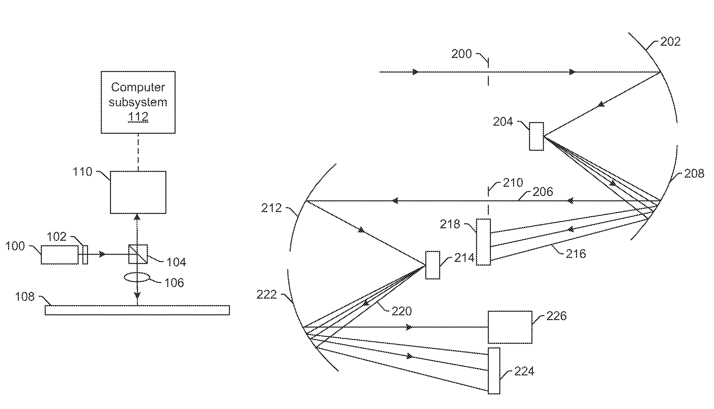
[0020]One embodiment relates to a system configured to determine information for a wafer. The system embodiments described herein can be used for optical metrology systems and applications, but may also be applied to inspection systems and applications. One embodiment of such a system is shown in FIG. 1. The system includes an illumination subsystem configured to direct light having wavelengths in a broadband (BB) range to a wafer. For example, as sh...


PUM


Abstract

Systems and methods for determining information for a wafer are provided. One system includes a first grating that diffracts light from a wafer having wavelengths in a first portion of a broadband range and does not diffract the light from the wafer having wavelengths in a second portion of the broadband range. The system also includes a second grating positioned in the path of the light that is not diffracted by the first grating. The second grating diffracts the light from the wafer having the wavelengths in the second portion of the broadband range. The system further includes a first detector configured to generate first output responsive to the light diffracted by the first grating and a second detector configured to generate second output responsive to the light diffracted by the second grating.

Description

BACKGROUND OF THE INVENTION[0001]1. Field of the Invention[0002]The present invention generally relates to systems and methods for determining information for wafers using selective diffraction with in-series gratings.[0003]2. Description of the Related Art[0004]The following description and examples are not admitted to be prior art by virtue of their inclusion in this section.[0005]Inspection and metrology processes are used at various steps during a semiconductor manufacturing process to detect defects on wafers and / or to measure one or more characteristics of the wafers to promote higher yield in the manufacturing process and thus higher profits. Inspection and metrology have always been important parts of fabricating semiconductor devices such as ICs. However, as the dimensions of semiconductor devices decrease, inspection and metrology become even more important to the successful manufacture of acceptable semiconductor devices because smaller defects and deviations can cause th...

Claims


Application Information

Patent Timeline
Patent Type & Authority Patents(United States)
IPC IPC(8): G01J3/28
CPCG01J3/28G01J3/36G01J3/18
Inventor FLOCK, KLAUS
Owner KLA CORP
Why Eureka
Try Eureka