Method for manufacturing SOI substrate

a technology of soi substrate and soi ions, which is applied in the direction of semiconductor/solid-state device manufacturing, basic electric elements, electric apparatus, etc., can solve the problems of uneven concentration distribution of hydrogen ions in silicon wafers, increase in surface unevenness, and not all hydrogen ions used for irradiation contribute to separation, etc., to achieve less surface unevenness and high crystallinity

Inactive Publication Date: 2014-11-04
SEMICON ENERGY LAB CO LTD
View PDF12 Cites 2 Cited by
  • Summary
  • Abstract
  • Description
  • Claims
  • Application Information

AI Technical Summary

Benefits of technology

[0014]In view of the foregoing, an object of one embodiment of the disclosed invention is to suppress desorption of hydrogen ions with which a single crystal semiconductor substrate is irradiated.
[0016]Furthermore, an object of one embodiment of the disclosed invention is to obtain an SOI substrate having a semiconductor layer with less surface unevenness.
[0018]The diffusion of hydrogen in crystalline silicon is accelerated by combination with excess interstitial silicon introduced by ion implantation or the like. Carbon is easily combined with such interstitial silicon; thus, diffusion of hydrogen can be suppressed.
[0032]According to one embodiment of the disclosed invention, desorption of hydrogen ions with which a single crystal semiconductor substrate is irradiated can be prevented.
[0033]Further, according to one embodiment of the disclosed invention, an SOI substrate having a semiconductor layer with high crystallinity can be obtained.
[0034]Furthermore, according to one embodiment of the disclosed invention, an SOI substrate having a semiconductor layer with less surface unevenness can be obtained.

Problems solved by technology

However, not all the hydrogen ions used for the irradiation contribute to the separation.
When the hydrogen ions used for the irradiation are diffused in the silicon wafer, concentration distribution of hydrogen ions in the silicon wafer is uneven.
This uneven concentration distribution of hydrogen ions in the silicon wafer causes a problem of an increase in surface unevenness of a semiconductor layer over a base substrate from which a part of the silicon wafer is separated.
In the case where heat treatment such as laser irradiation or the like is performed to recover crystallinity of the semiconductor layer over the base substrate from which the part of the silicon wafer is separated, there is a possibility that a defect, dislocation, or the like remains in the semiconductor layer irradiated with a large number of hydrogen ions even after the heat treatment and crystallinity is not recovered sufficiently.
If a semiconductor device is manufactured using a semiconductor layer of which crystallinity is not recovered, characteristics of the semiconductor device may be degraded.
Further, in the case where the surface unevenness of the semiconductor layer over the base substrate from which the part of the silicon wafer is separated increases as described above, a void may be produced on the surface of the semiconductor layer when the heat treatment such as laser irradiation or the like is performed.

Method used


Image

  • Method for manufacturing SOI substrate
  • Method for manufacturing SOI substrate
  • Method for manufacturing SOI substrate

Examples


embodiment 1

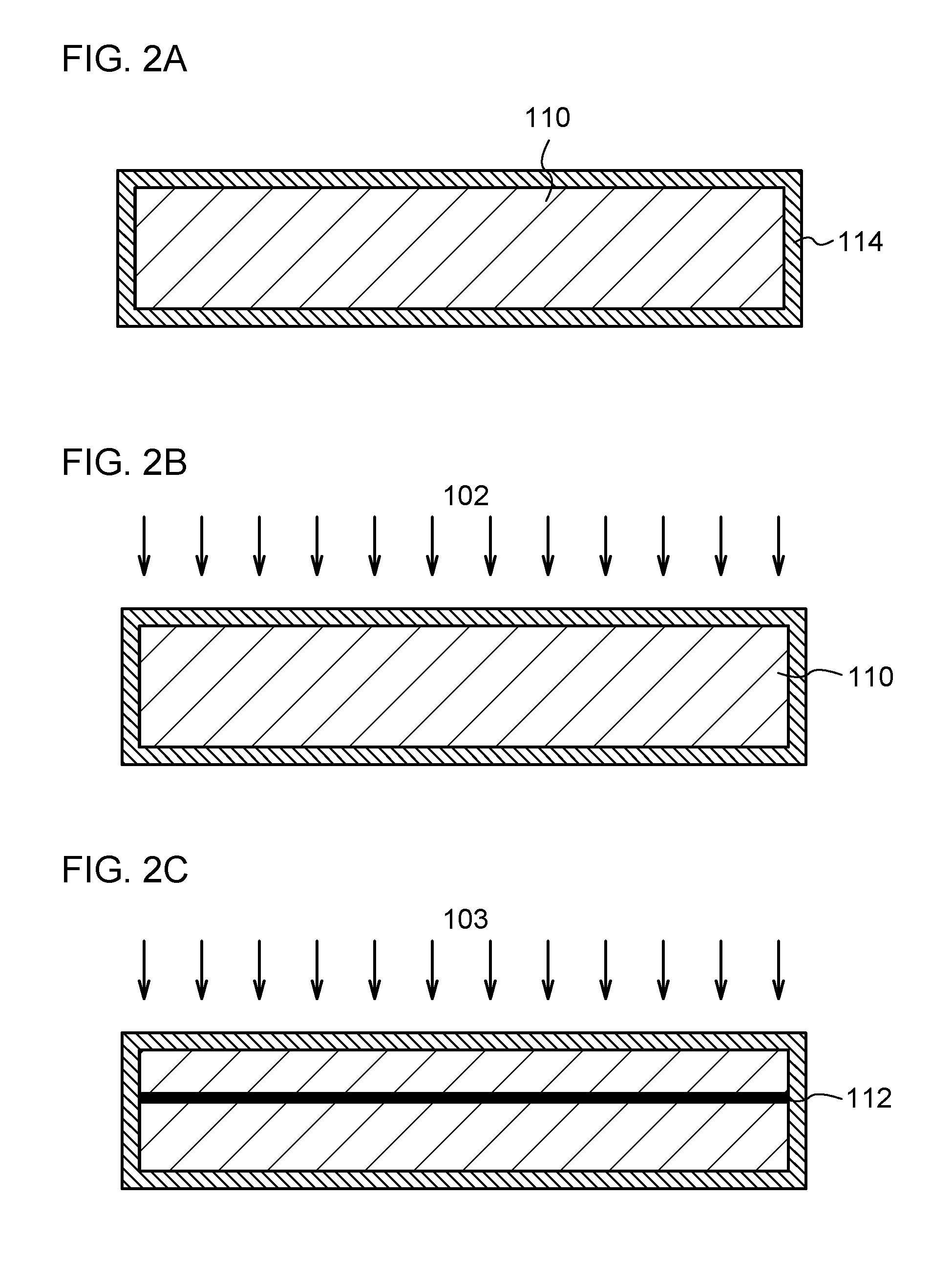
[0042]First, a semiconductor substrate 110 is prepared as a bond substrate. A polycrystalline semiconductor substrate or a single crystal semiconductor substrate can be used as the semiconductor substrate 110. As the semiconductor substrate 110, for example, a semiconductor substrate that is formed of an element which belongs to Group 14, such as a polycrystalline or single crystal silicon substrate, a polycrystalline or single crystal germanium substrate, a polycrystalline or single crystal silicon germanium substrate, or a polycrystalline or single crystal silicon carbide substrate; or a polycrystalline or single crystal compound semiconductor substrate using gallium arsenide, indium phosphide, or the like can be given. The size of a silicon substrate is typically 5 inches (125 mm) in diameter, 6 inches (150 mm) in diameter, 8 inches (200 mm) in diameter, and 12 inches (300 mm) in diameter, and a typical shape thereof is a circular shape. Note that the shape of the silicon substra...

embodiment 2

[0100]In this embodiment, a method for manufacturing an SOI substrate, which is different from that shown in Embodiment 1 will be described. Only an aspect different from Embodiment 1 is described in this embodiment. A portion which is not described in this embodiment follows the description in Embodiment 1.

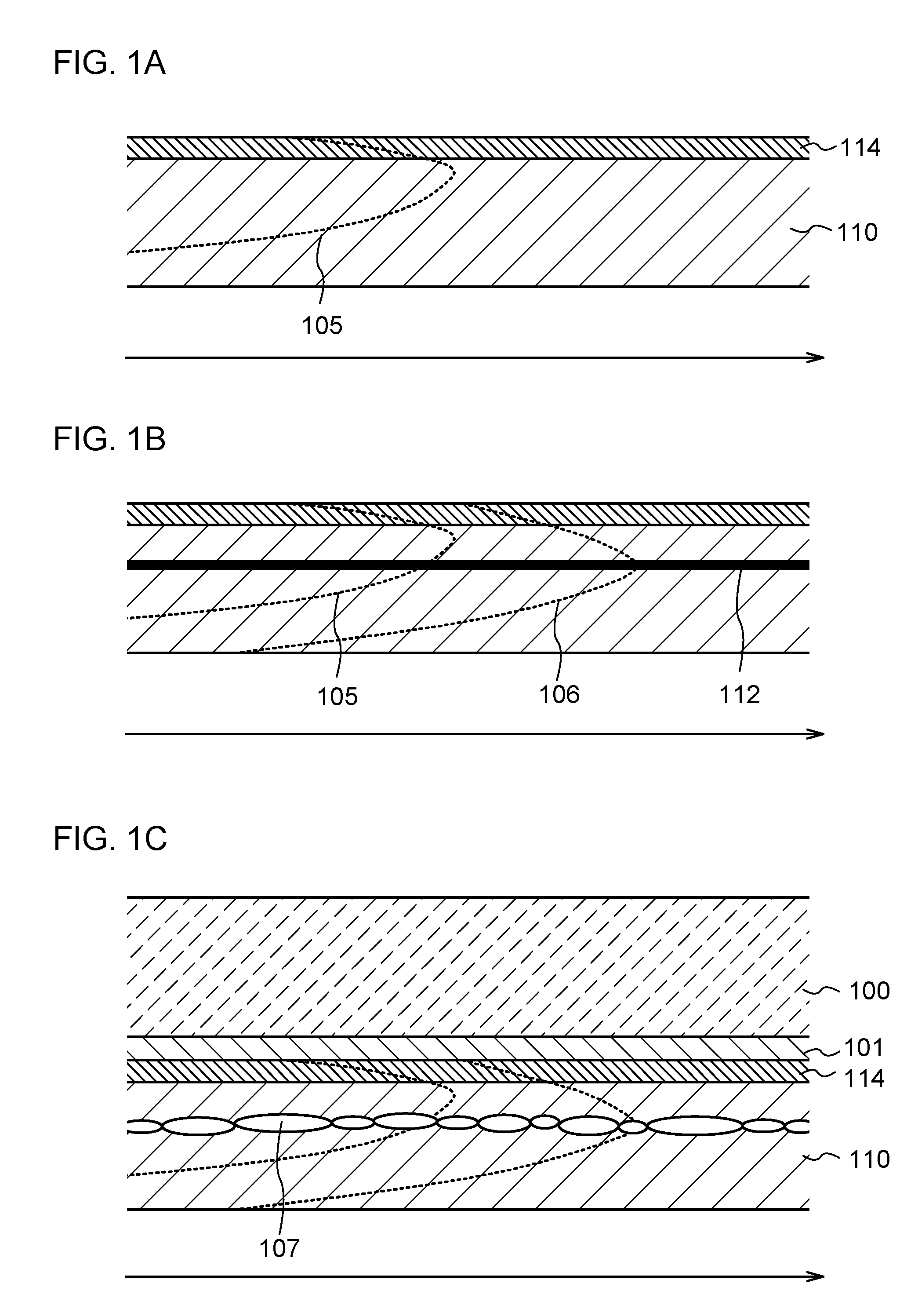
[0101]In this embodiment, instead of the carbon ions 102 described in Embodiment 1, cluster ions (CHxHy+) including carbon and hydrogen are used for the irradiation. In the case where the cluster ions (CHxHy+) including carbon and hydrogen are used, carbon and hydrogen can be added at the same time; thus, the hydrogen micro-bubbles 107 can be formed further effectively.

[0102]In the case where the semiconductor substrate 110 is irradiated with the cluster ions including carbon and hydrogen, for example, a dose of the cluster ions may be 1×10¹⁵ ions / cm2. The acceleration voltage is changed depending on the value of x. For example, when x is 1, the acceleration voltage may be higher...

embodiment 3

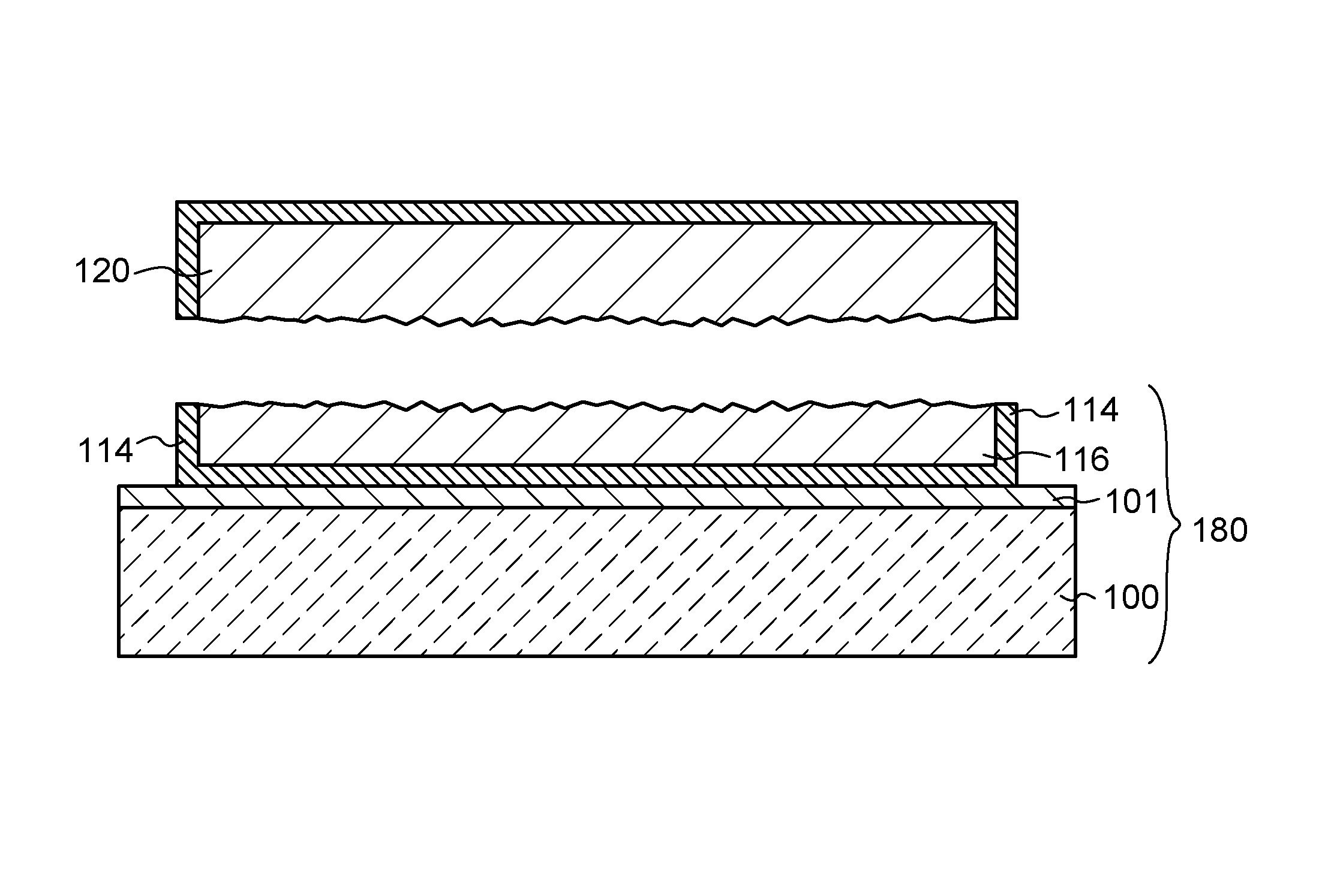
[0109]FIG. 4A is a cross-sectional view illustrating part of the SOI substrate manufactured by the method described in Embodiments 1 and 2 (see FIG. 3C).

[0110]In order to control the threshold voltage of a thin film transistor (TFT), a p-type impurity such as boron, aluminum, or gallium, or an n-type impurity such as phosphorus or arsenic may be added to the semiconductor layer 118. A region to which the impurity is added and the kind of impurity to be added can be changed as appropriate. For example, a p-type impurity is added to a formation region of an n-channel TFT, and an n-type impurity is added to a formation region of a p-channel TFT. The above impurity elements may be added at a dose of approximately greater than or equal to 1×10¹¹ ions / cm2 and lower than or equal to 1×10¹⁴ ions / cm2.

[0111]Then, the semiconductor layer 118 is divided into island shapes to form a semiconductor layer 122 and a semiconductor layer 124 (see FIG. 4B).

[0112]Next, an insulating film 126 is formed t...


PUM

PropertyMeasurementUnit
diameteraaaaaaaaaa
diameteraaaaaaaaaa
sizeaaaaaaaaaa

Abstract

To suppress desorption of hydrogen ions with which a single crystal semiconductor substrate is irradiated. A method for manufacturing an SOI substrate includes the following steps: irradiating a semiconductor substrate with carbon ions; irradiating the semiconductor substrate with a hydrogen ion after the irradiation with the carbon ion so as to form an embrittled region in the semiconductor substrate; disposing a surface of the semiconductor substrate and a surface of a base substrate to face each other and to be in contact with each other so that the semiconductor substrate and the base substrate are bonded; and heating the semiconductor substrate and the base substrate which are bonded to each other and separating the semiconductor substrate along the embrittled region so that a semiconductor layer is formed over the base substrate.

Description

BACKGROUND OF THE INVENTION[0001]1. Field of the Invention[0002]One embodiment of the disclosed invention relates to a method for manufacturing an SOI substrate.[0003]2. Description of the Related Art[0004]In recent years, an integrated circuit using an SOI (silicon on insulator) substrate in which a thin single crystal semiconductor layer is formed on an insulating surface, instead of a bulk silicon wafer, has been developed. The use of an SOI substrate can reduce parasitic capacitance between a drain of a transistor and a substrate; thus, SOI substrates are attracting attention for their ability to improve performance of semiconductor integrated circuits.[0005]One of known methods for manufacturing SOI substrates is a hydrogen ion implantation separation method (for example, see Patent Document 1). A summary of a method for manufacturing an SOI substrate by a hydrogen ion implantation separation method is as follows. First, hydrogen ions are implanted into a silicon wafer by an io...

Claims


Application Information

Patent Timeline
Patent Type & Authority Patents(United States)
IPC IPC(8): H01L21/762
CPCH01L21/76254
Inventor KOEZUKA, JUNICHI
Owner SEMICON ENERGY LAB CO LTD
Why Eureka
Try Eureka