Eureka AIR delivers breakthrough ideas for toughest innovation challenges, trusted by R&D personnel around the world.

Flash memory and layout method thereof

Active Publication Date: 2014-11-11
WINBOND ELECTRONICS CORP
View PDF2 Cites 0 Cited by
  • Summary
  • Abstract
  • Description
  • Claims
  • Application Information

AI Technical Summary

Benefits of technology

The patent is about a flash memory that has a core array to store data, a peripheral circuit to access the data, an off-chip driver to process the data, an interconnect structure to connect them, and an uppermost conductive layer with a power pad and tracks to transmit power to the other components. The technical effect of this invention is to enable efficient and reliable power supply to the core array, peripheral circuit, and off-chip driver through the interconnect structure.

Problems solved by technology

As technological developments advance, the size of flash memory is becoming smaller and smaller, due in large part to the thickness of the metal layers in the flash memory becoming thinner and thinner.
Since the metal lines in the metal layers are configured to transmit power, the power can be easily interfered by noise.

Method used


Image

  • Flash memory and layout method thereof
  • Flash memory and layout method thereof
  • Flash memory and layout method thereof

Examples


Embodiment Construction

[0014]The following description is of the best-contemplated mode of carrying out the invention. This description is made for the purpose of illustrating the general principles of the invention and should not be taken in a limiting sense. The scope of the invention is best determined by reference to the appended claims.

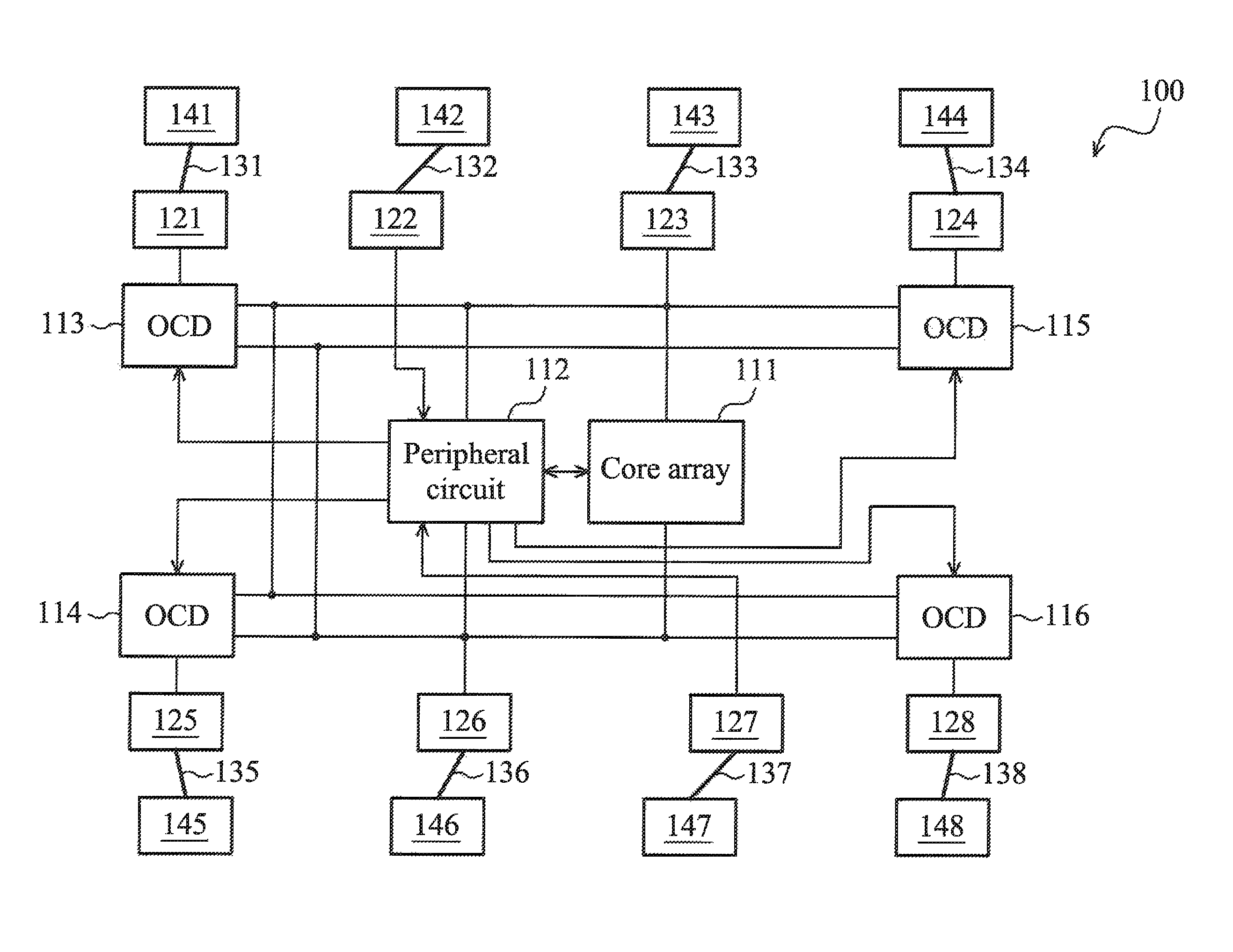
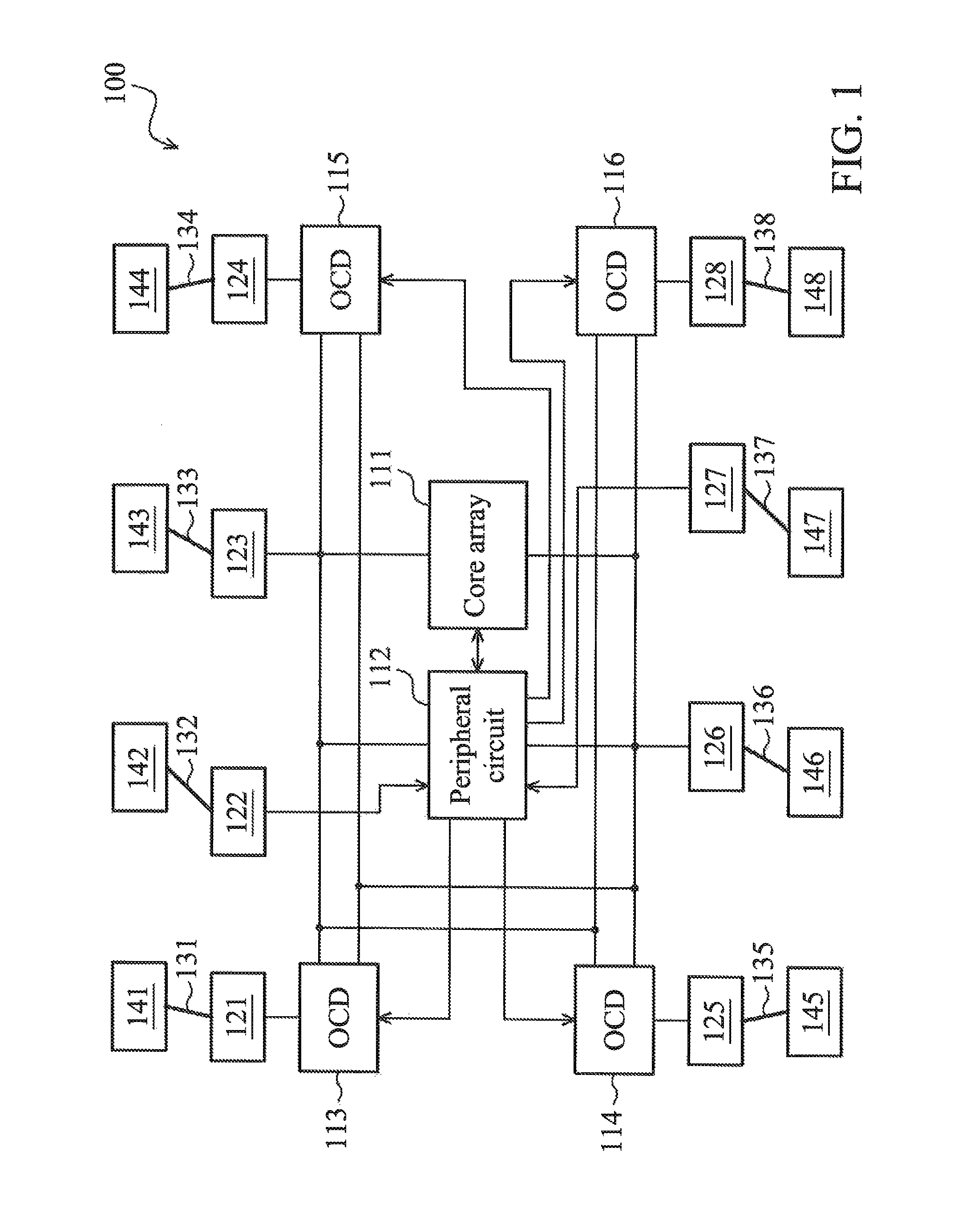
[0015]FIG. 1 is a structure diagram of an exemplary embodiment of a flash memory in accordance with some embodiments. The flash memory 100 comprises a core array 111, a peripheral circuit 112, off-chip drivers (OCDs) 113-116 and pads 121-128.

[0016]The core array 111 comprises memory cells (not shown) for storing data. In some embodiments, the memory cells are arranged to form an array. The disclosure does not limit the circuit structure of the memory cells. Any circuit can serve as the core array 111, as long as the circuit is capable of storing data. In some embodiments, the core array 111 operates according to an operation voltage received by the pads 123 and 126.

[00...


PUM


Abstract

A flash memory is disclosed. A core array stores data. A peripheral circuit accesses the data stored in the core array to generate read data. A off-chip driver (OCD) processes the read data to generate output data. An interconnect structure is electrically connected to the core array, the peripheral circuit, and the OCD and includes three conductive layers. The conductive layers are electrically connected to each other. An uppermost conductive layer is formed over the interconnect structure, electrically connected to the interconnect structure, and includes a first power pad and first power tracks. The first power pad is electrically connected to a power pin via a first bonding wire to receive an operation voltage. The first power tracks are electrically connected between the first power pad and the interconnect structure to transmit the operation voltage to at least one of the core array, the peripheral circuit and the OCD.

Description

BACKGROUND OF THE INVENTION[0001]1. Field of the Invention[0002]The invention relates to a memory, and more particularly to a flash memory.[0003]2. Description of the Related Art[0004]Flash memories are non-volatile memories and are widely used in personal digital assistants (PDAs), notebooks (NBs), walkmans, digital still cameras (DSCs) and mobile phones. As technological developments advance, the size of flash memory is becoming smaller and smaller, due in large part to the thickness of the metal layers in the flash memory becoming thinner and thinner. Since the metal lines in the metal layers are configured to transmit power, the power can be easily interfered by noise.BRIEF SUMMARY OF THE INVENTION[0005]In accordance with an embodiment, a flash memory comprises a core array, a peripheral circuit, an off-chip driver (OCD), an interconnect structure and an uppermost conductive layer. The core array stores data. The peripheral circuit accesses the data stored in the core array to g...

Claims


Application Information

Patent Timeline
IPC IPC(8): H01L23/52G11C5/06G11C16/26G11C5/02H01L21/768
CPCH01L21/768G11C16/26G11C5/06G11C5/025G11C5/063G11C16/30
Inventor YEH, JUN-LINYEN, TING-KUO
Owner WINBOND ELECTRONICS CORP
Why Eureka
Eureka Blog
Learn More