Pixel structure of organic light emitting display device

a technology of light-emitting display device and pixel structure, which is applied in the direction of light-emitting support device, discharge tube luminescnet screen, instruments, etc., can solve the problems of complicated manufacturing process of masks and worse stability of organic light-emitting materials, and achieve low precision demands on masks and improved manufacturing process stability.

Inactive Publication Date: 2014-11-25
CHUNGHWA PICTURE TUBES LTD
View PDF7 Cites 34 Cited by
  • Summary
  • Abstract
  • Description
  • Claims
  • Application Information

AI Technical Summary

Benefits of technology

[0006]It is one of the objectives of the present invention to provide a pixel structure of an organic light emitting display device. A sub-pixel in each display pixel unit and tree adjacent sub-pixels in the same color are disposed adjacently to one another to compose a pixel unit. Purposes of low precision demands on masks and improved manufacturing process stability may be achieved accordingly.

Problems solved by technology

Problems such as complicated manufacturing process of the masks and worse stability of the organic light emitting material may become serious accordingly.

Method used


Image

  • Pixel structure of organic light emitting display device
  • Pixel structure of organic light emitting display device
  • Pixel structure of organic light emitting display device

Examples


Embodiment Construction

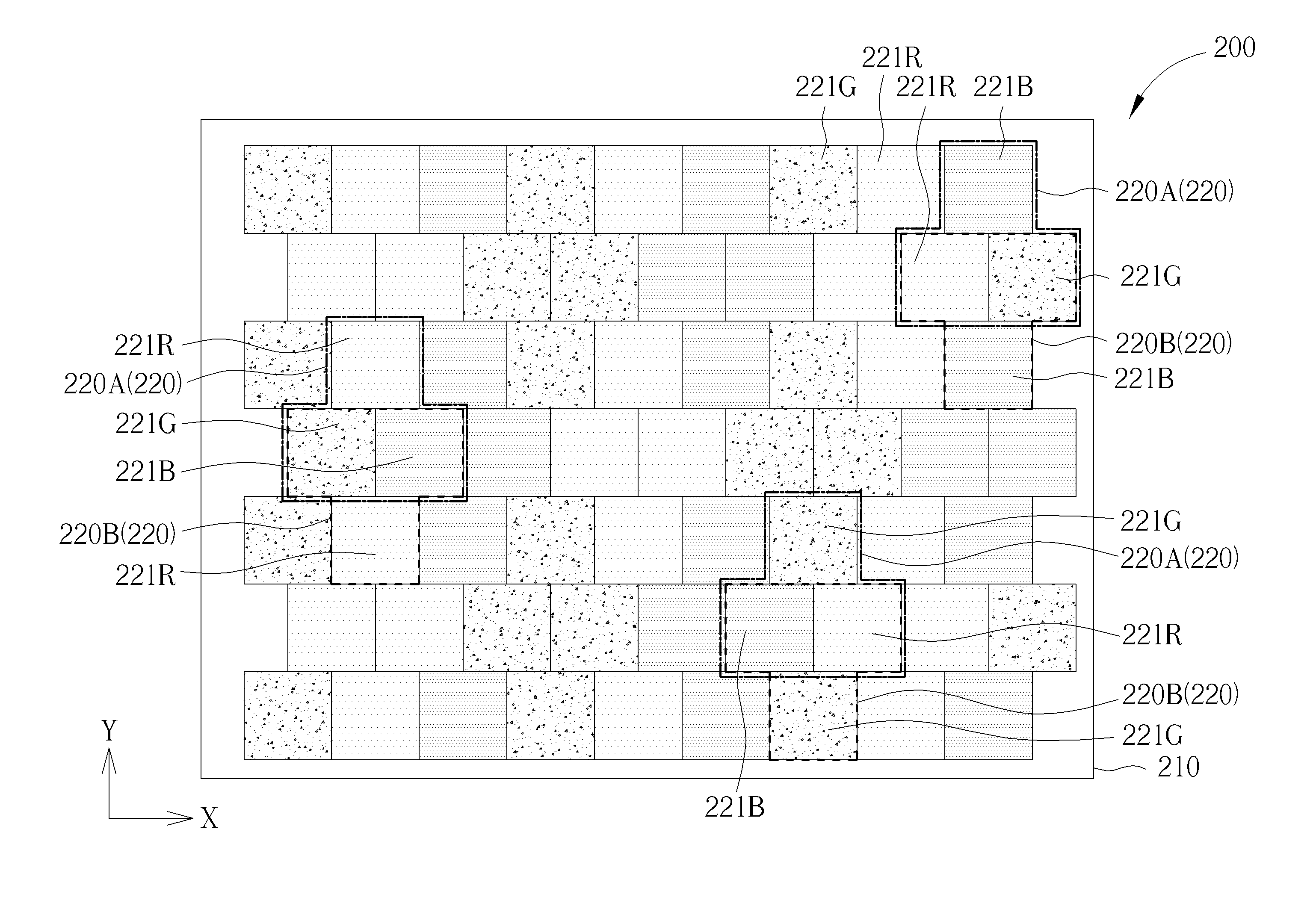
[0018]Please refer to FIGS. 3-5. FIG. 3 is a schematic diagram illustrating a pixel structure of an organic light emitting display device according to a first preferred embodiment of the present invention. FIG. 4 is a schematic diagram illustrating an arrangement of display pixel units in the pixel structure of the organic light emitting display device according to this embodiment. FIG. 5 is a schematic diagram illustrating a mask in this embodiment. Please note that the figures are only for illustration and the figures may not be to scale. The scale may be further modified according to different design considerations. As shown in FIG. 3 and FIG. 4, a pixel structure 200 of an organic light emitting display device is provided in this embodiment. The pixel structure 200 includes a substrate 210 and a plurality of display pixel units 220. The display pixel units 220 are disposed on the substrate 210. Each of the display pixel units 220 includes a first sub-pixel 221R, a second sub-pix...


PUM


Abstract

A pixel structure of an organic light emitting display device includes a substrate and a plurality of display pixel units disposed on the substrate. Each of the display pixel units includes a first sub-pixel, a second sub-pixel and a third sub-pixel disposed adjacently to one another. The first sub-pixel in each of the display pixel units is disposed adjacently to three first sub-pixels respectively disposed in three adjacent display pixel units to form a first pixel unit. The second sub-pixel in each of the display pixel units is disposed adjacently to three second sub-pixels respectively disposed in three adjacent display pixel units to form a second pixel unit. The third sub-pixel in each of the display pixel units is disposed adjacently to three third sub-pixels respectively disposed in three adjacent display pixel units to form a third pixel unit.

Description

BACKGROUND OF THE INVENTION[0001]1. Field of the Invention[0002]The present invention relates to a pixel structure of an organic light emitting display device and more particularly, to a pixel structure where allocations of the sub-pixels are modified for lowering demands on precisions of masks and enhancing manufacturing process stability of the pixel structure.[0003]2. Description of the Prior Art[0004]Organic light emitting diode displays, which have the advantages of absence of color filter, self-luminescence and low power consumption, is always viewed as the best candidate to substitute for the liquid crystal display and become the main display technology of the next generation.[0005]Please refer to FIG. 1 and FIG. 2. FIG. 1 is a schematic diagram illustrating a conventional organic light emitting diode display device. FIG. 2 is a schematic diagram illustrating a mask used for manufacturing the conventional organic electroluminescent display device. As shown in FIG. 1 and FIG. ...

Claims


Application Information

Patent Timeline
Patent Type & Authority Patents(United States)
IPC IPC(8): H01L51/52F21V21/00
CPCF21V21/00G09F13/00H01L27/32H01L27/3218H10K59/353
Inventor HUANG, SZU-CHIHUANG, CHIN-HAISUN, BO-JHANG
Owner CHUNGHWA PICTURE TUBES LTD
Why Eureka
Try Eureka