
Liquid crystal display, control method thereof and electronic device with reduced flicker

a technology of electronic devices and liquid crystal displays, applied in the direction of instruments, computing, electric digital data processing, etc., can solve the problem of difficult to detect transmittance accurately, and achieve the effect of suppressing the application of dc components and reducing flicker

Inactive Publication Date: 2014-12-09
SEIKO EPSON CORP
View PDF10 Cites 2 Cited by
  • Summary
  • Abstract
  • Description
  • Claims
  • Application Information

AI Technical Summary

Benefits of technology

[0007]An advantage of some aspects of the invention is to provide a technique capable of suppressing application of a DC component to a liquid crystal layer and reducing flicker, without employing a light sensing element.
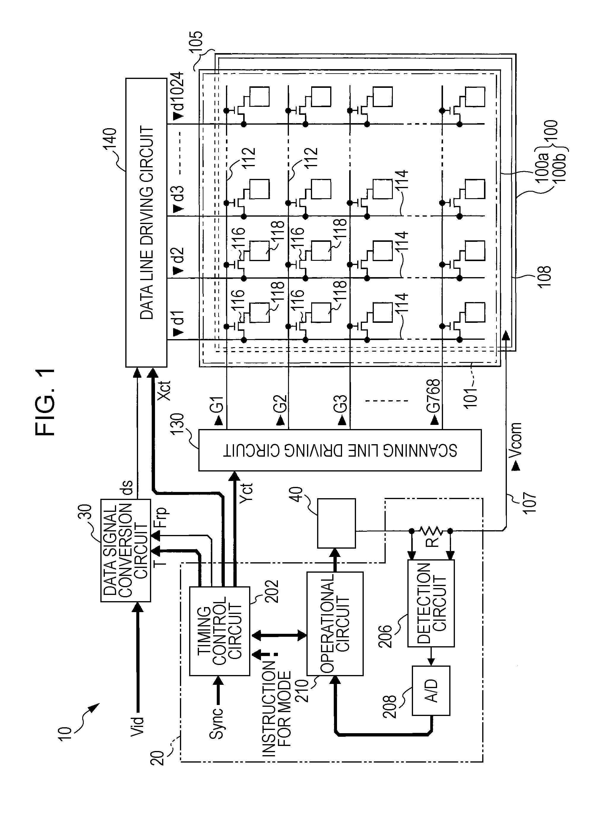
[0008]An LCD according to an embodiment of the invention includes liquid crystal elements in which a liquid crystal layer is sandwiched by a first electrode and a second electrode; a driving circuit configured to alternately apply higher and lower voltages than a predetermined voltage to the first electrode, and, at the same time, to apply the predetermined voltage to the second electrode; and a control circuit configured to compare a first current with a second current, the first current being obtained by excluding an instantaneous current due to application of a related higher voltage from currents flowing through the second electrode after the higher voltage is applied to the first electrode, and the second current being obtained by excluding an instantaneous current due to application of a related lower voltage from currents flowing through the second electrode after the lower voltage is applied to the first electrode, and to control the predetermined voltage based on the comparison result. According to the invention, it is possible to suppress the application of a DC component to the liquid crystal layer and to reduce flicker without employing a light sensing element.
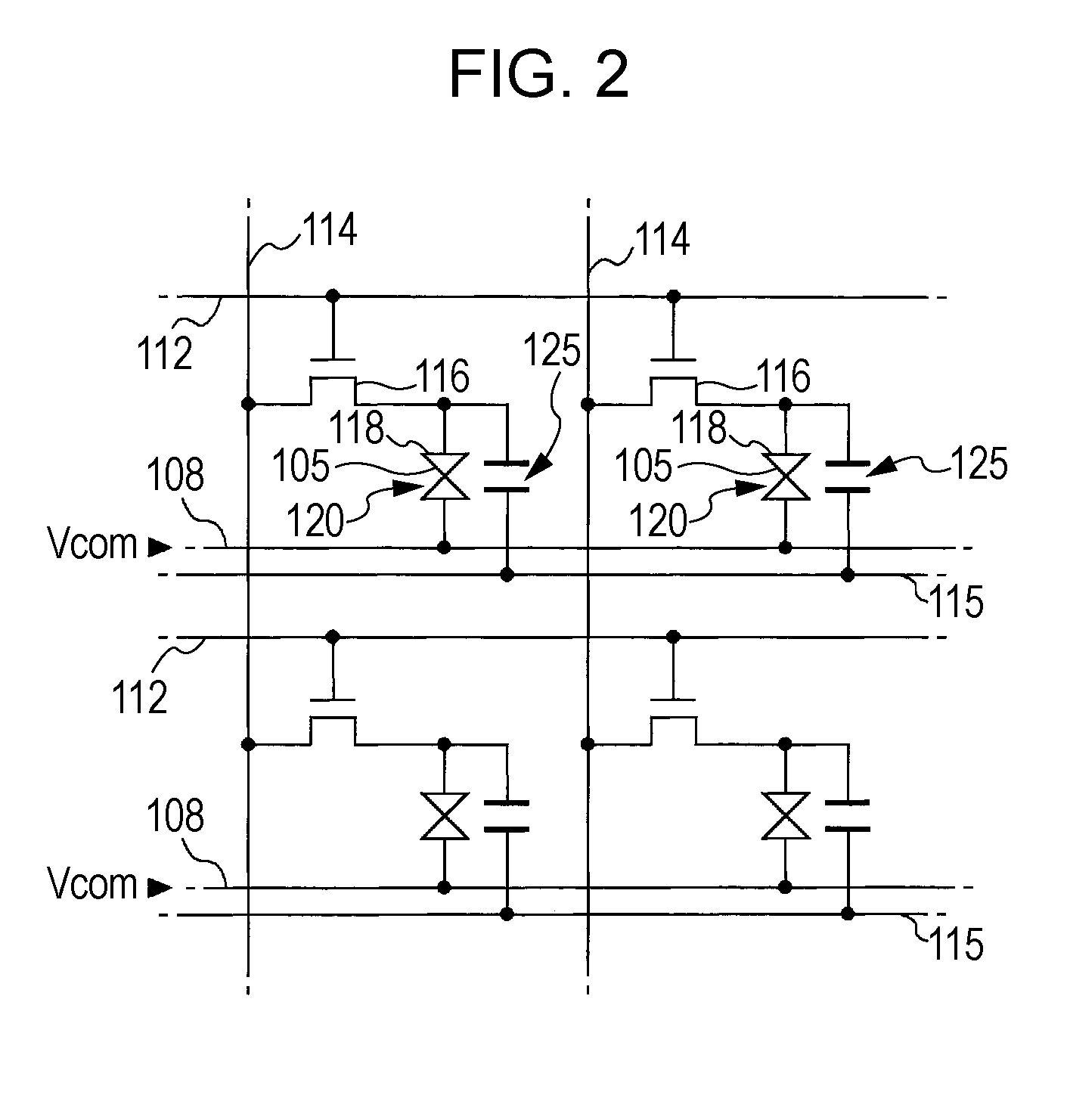
[0012]In the meantime, the first electrode may be a pixel electrode which is coupled to a data line via a switching element, which is turned on when a scanning line is selected, and the second electrode may be a common electrode. The driving circuit may include a scanning line driving circuit selecting the scanning line, a data line driving circuit supplying a data signal for the data line at the selection period, and a common electrode driving circuit supplying the predetermined voltage for the common electrode, and wherein the control circuit may increase or decrease the predetermined voltage. In this configuration, the scanning line driving circuit may select the scanning line and thereafter not select the related scanning line by turning off the switching element. Thereby, it is possible to suppress the application of a DC component to the liquid crystal layer, also in consideration of a state where the switching element is turned off.

Problems solved by technology

However, if the light sensing element is formed, there are problems in that it has bad influence on the viewability of display images or a so-called frame is broadened, and there are also problems in that stray light inside the display device enters the light sensing element and thereby it is difficult to detect the transmittance accurately.

Method used


Image

  • Liquid crystal display, control method thereof and electronic device with reduced flicker
  • Liquid crystal display, control method thereof and electronic device with reduced flicker
  • Liquid crystal display, control method thereof and electronic device with reduced flicker

Examples


first embodiment

[0027]To begin with, a first embodiment of the invention will be described in outline.

[0028]In order to prevent seizing or deterioration of liquid crystal, an AC driving is required to be performed for a liquid crystal element in which a liquid crystal layer is sandwiched by a first electrode and a second electrode. For example, a voltage with positive polarity higher than a reference voltage (higher voltage) and a voltage with negative polarity lower than the reference voltage (lower voltage) are alternately applied to the first electrode, while a predetermined voltage is applied to the second electrode. At this time, if transmittance (or reflectance) in the liquid crystal element at a period where the voltage is applied and kept positive is different from that in the liquid crystal element at a period where the voltage is applied and kept negative, this makes flicker (blink) recognized.

[0029]Liquid crystal molecules alter their inclined arrangement depending on the electric field ...

second embodiment

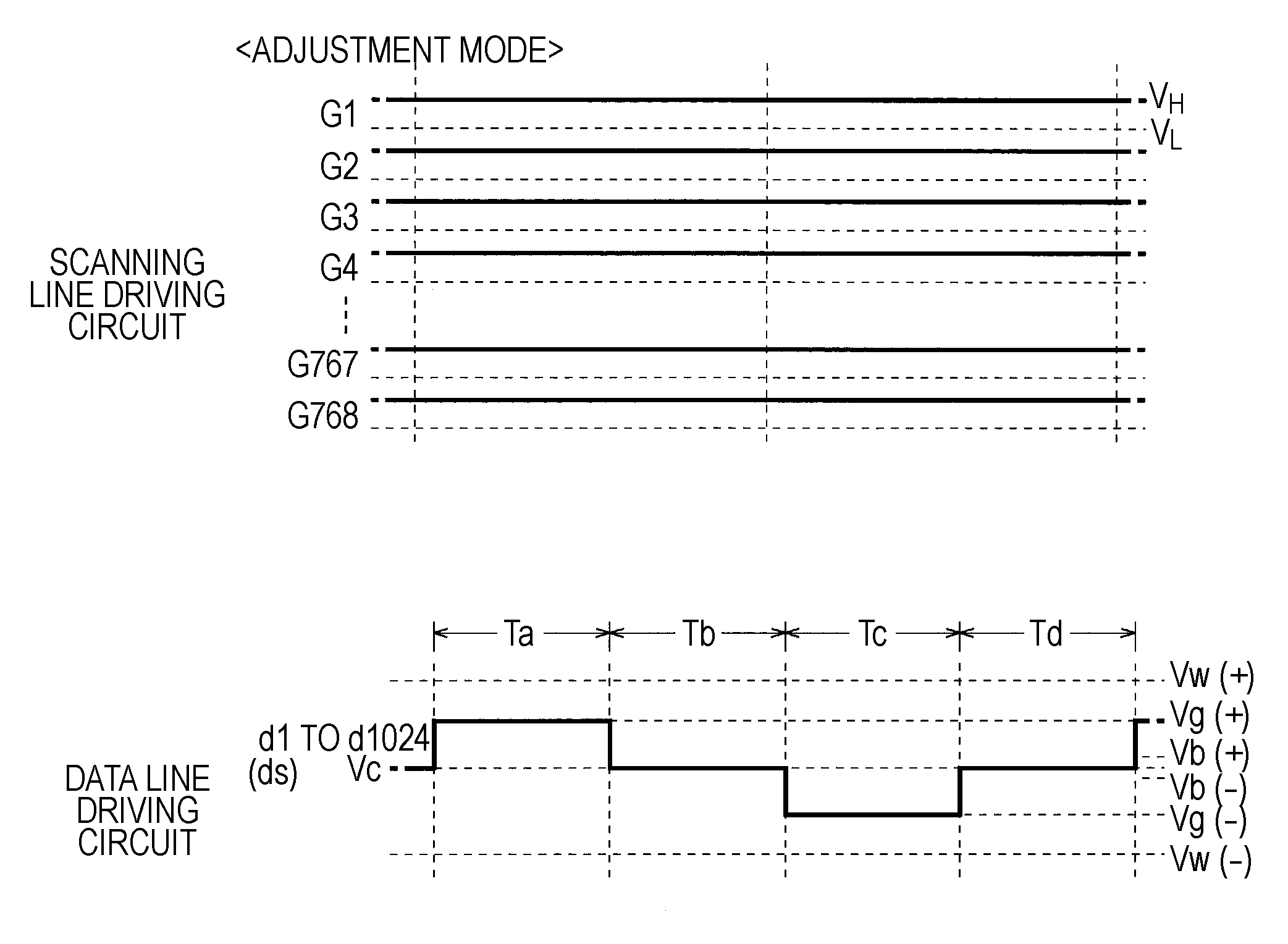
[0116]Next, a second embodiment of the invention will be described. The second embodiment is the same as the first embodiment except that waveforms for the scanning signals G1 to G768 in the adjustment mode in the first embodiment are as shown in FIG. 7A.

[0117]In detail, in the adjustment mode in the second embodiment, the scanning signals G1 to G768 have the H level only for the time s from the start timings of the respective durations Ta, Tb, Tc, and Td and the L level for the remaining time.

[0118]As described above, the driving voltage for the liquid crystal element 120 is instantaneously varied relative to the voltage applied to the pixel electrode 118, and thereby although the scanning signal has the H level only for the time s, the difference between the voltage of the data signal and the voltage of the common signal is enough to be maintained in the liquid crystal elements 120.

[0119]Meanwhile, in the display mode, when the TFT 116 is turned on and thereafter turned off, there...

third embodiment

[0123]A third embodiment of the invention will be described. In this third embodiment, as shown in FIG. 8, an LPF (low pass filter) 207 which passes only a low frequency component of the output signal of the detection circuit 206 is employed, and further the scanning line driving circuit 130 performs a line sequential driving in which the scanning lines are selected in the same order as the display mode without differentiation depending on the operation modes, as shown in FIG. 9A.

[0124]In such a line sequential driving, the waveform of the current flowing through the signal line 107 (more accurately, the waveform of the voltage converted from the current) is obtained by overlapping the respective current waveforms caused by the selection of each scanning line, that is, the respective current waveforms appearing when the scanning signals G1, G2, G3, . . . , and G768 become the H level, as shown in FIG. 9B wherein the current waveform is determined by a selection of each row. The inst...


PUM


Abstract

A liquid crystal display includes liquid crystal elements in which a liquid crystal layer is sandwiched by a first electrode and a second electrode, a driving circuit configured to alternately apply higher and lower voltages than a predetermined voltage to the first electrode, and, at the same time, to apply the predetermined voltage to the second electrode, and a control circuit configured to compare a first current with a second current, the first current being obtained by excluding an instantaneous current due to a related higher voltage from currents flowing through the second electrode after the higher voltage is applied to the first electrode, and the second current being obtained by excluding an instantaneous current due to a related lower voltage from currents flowing through the second electrode after the lower voltage is applied to the first electrode, and to control the predetermined voltage based on the comparison result.

Description

BACKGROUND[0001]1. Technical Field[0002]The present invention relates to a technique which can prevent flicker or the like in a liquid crystal display.[0003]2. Related Art[0004]Liquid crystal elements, which can be used in a liquid crystal display (“LCD”), enable a liquid crystal layer to be sandwiched by two electrodes, but the liquid crystal layer is applied with a direct current (“DC”) component, which deteriorates the liquid crystal layer. For this reason, in the LCD, an alternating current (“AC”) driving is performed in which one electrode is alternately applied with a higher voltage and a lower voltage than a voltage applied to the other electrode.[0005]A difference in the voltage effective values at this time makes flicker recognized, and a technique is known which prevents the deterioration of the liquid crystal layer by forming a light sensing element such as a photodiode or the like on a panel or in the vicinity thereof and further by adjusting the voltage applied to the o...

Claims


Application Information

Patent Timeline
Patent Type & Authority Patents(United States)
IPC IPC(8): G09G3/36G09G5/00
CPCG09G3/3648G09G2300/0876G09G2320/0247G09G2310/061G09G2320/0204
Inventor MIZUSAKO, KAZUHISA
Owner SEIKO EPSON CORP
Learn More