Light emitting device

a technology of light emitting diodes and light emitting diodes, which is applied in the direction of semiconductor devices, basic electric elements, electrical equipment, etc., can solve the problems of inconvenient trouble of conventional light emitting diodes by direct current, and the inability to apply conventional light emitting diodes in dc-driven environments, so as to increase the total light emitting efficiency of light emitting devices and increase the light reflection

Active Publication Date: 2014-12-23
GENESIS PHOTONICS
View PDF7 Cites 2 Cited by
  • Summary
  • Abstract
  • Description
  • Claims
  • Application Information

AI Technical Summary

Benefits of technology

[0008]The invention provides a light emitting device, which is capable of increasing the light reflection effect at the bridging portion of the two adjacent light emitting diodes, so as to increase the total light emitting efficiency of the light emitting device.
[0029]Based on the above description, the reflective layer of the invention not only has electrical capability so as to electrically connect the two adjacent light emitting diodes, but also has high reflective efficiency so as to reflect beams emitted from the light emitting layers of the light emitting diodes. Therefore, compared with the conventional HV LED, the light emitting device has better light emitting efficiency.

Problems solved by technology

Since the conventional light emitting diodes are driven by direct current (DC), the conventional light emitting diodes can only be applied in DC-driven environments.
Therefore, there exists an inconvenient trouble of the conventional light emitting diodes by using direct current.

Method used


Image

  • Light emitting device
  • Light emitting device
  • Light emitting device

Examples


Embodiment Construction

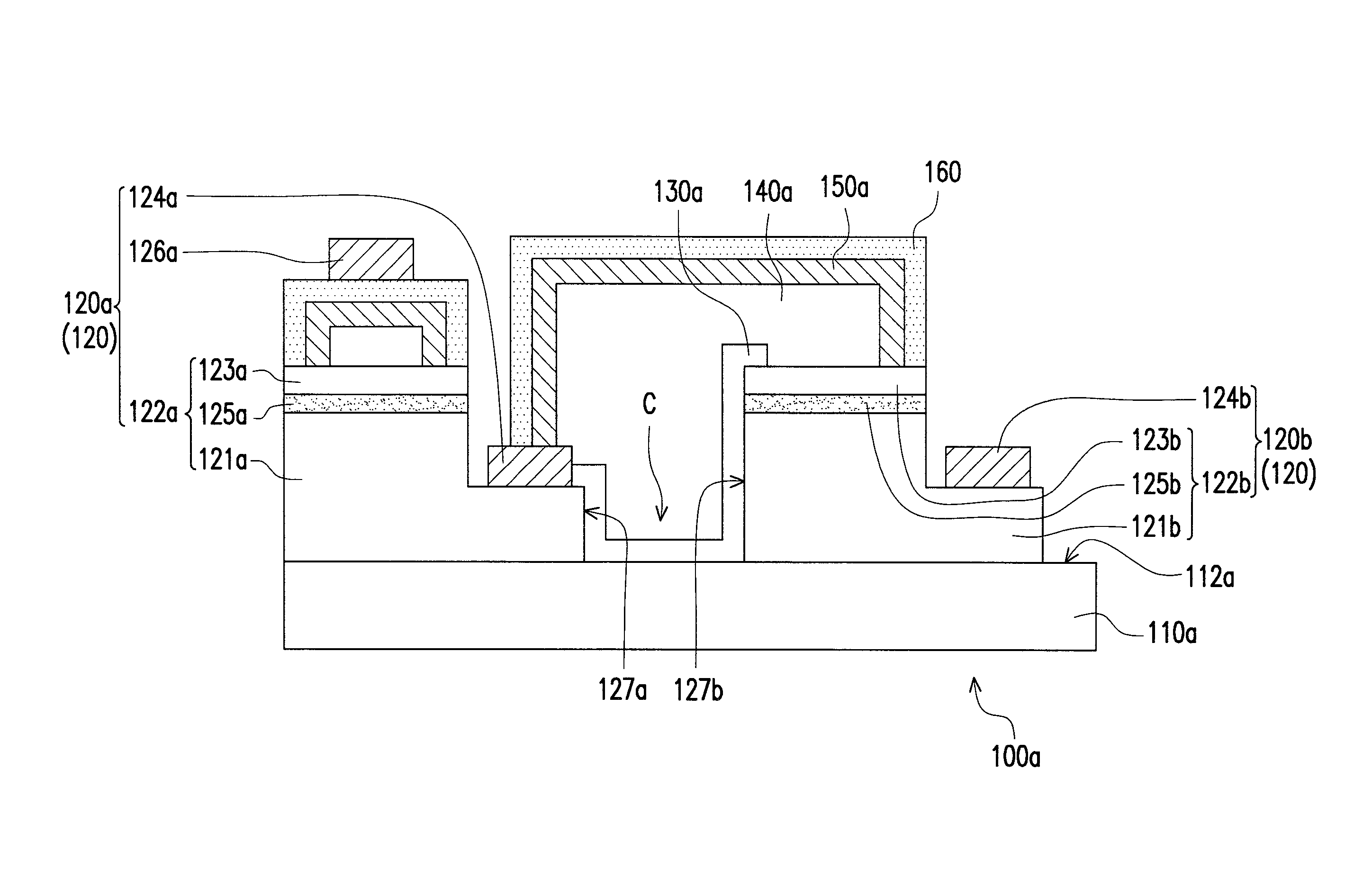
[0037]FIG. 1 is a schematic cross-sectional view illustrating a light emitting device according to an embodiment of the present invention. Referring to FIG. 1, in this embodiment, the light emitting device 100a includes a substrate 110a, light emitting units 120, an insulation layer 130a, a current distribution layer 140a, and a reflective layer 150a. The substrate 110a has an upper surface 112a. The light emitting units 120a are disposed on the upper surface 112a of the substrate 110a. The light emitting units 120 includes at least one first light emitting diode 120a (FIG. 1 schematically illustrates only one) and at least one second light emitting diode 120b (FIG. 1 schematically illustrates only one). A first side wall 127a of the first light emitting diode 120a and a second side wall 127b of the second light emitting diode 120b are adjacent and define a concave portion C, and the concave portion C exposes a portion of the upper surface 112a of the substrate 110a. The insulation ...


PUM


Abstract

A light emitting device includes a substrate, light emitting units, an insulation layer, a current distribution layer and a reflective layer. The substrate has an upper surface. The light emitting units are disposed on the upper surface and include at least one first light emitting diode (LED) and at least one second LED. A first side wall of the first LED is adjacent to a second side wall of the second LED so as to define a concave portion exposing a portion of the upper surface. The insulation layer at least covers the first side wall and the second side wall. The current distribution layer covers the concave portion and at least covers a portion of the second LED. The reflective layer covers the current distribution layer and is electrically connected to the first LED and the second LED.

Description

CROSS-REFERENCE TO RELATED APPLICATION[0001]This application claims the priority benefit of Taiwan application serial no. 101148146, filed on Dec. 18, 2012. The entirety of the above-mentioned patent application is hereby incorporated by reference herein and made a part of this specification.BACKGROUND OF THE INVENTION[0002]1. Field of the Invention[0003]The invention relates to a light emitting device, and more particularly, to a light emitting device using a light emitting diode as light source.[0004]2. Description of Related Art[0005]As the technology for light emitting diode (LED) grows, light emitting diodes have gradually taken the place of traditional bulbs in lighting field. Since the conventional light emitting diodes are driven by direct current (DC), the conventional light emitting diodes can only be applied in DC-driven environments. Or, AC-DC converters and voltage transformers are needed for transferring the conventional alternating current (AC) to the lower voltage di...

Claims


Application Information

Patent Timeline
Patent Type & Authority Patents(United States)
IPC IPC(8): H01L33/44H01L33/20H01L33/40H01L33/36H01L33/10H01L33/46H01L33/62H01L27/15
CPCH01L33/10H01L33/46H01L33/62H01L33/405H01L2924/0002H01L33/44H01L33/20H01L33/36H01L33/40H01L27/153H01L2924/00
Inventor HUANG, JING-ENHUANG, YI-RUWU, CHIH-LINGLO, YU-YUN
Owner GENESIS PHOTONICS
Why Eureka
Try Eureka