Regulation of memory IO timing using programmatic control over memory device IO timing
a technology of memory devices and io timing, applied in the direction of instruments, data conversion, generating/distributing signals, etc., can solve the problems of reducing overall power, highest power consumption, and reducing power savings
- Summary
- Abstract
- Description
- Claims
- Application Information
AI Technical Summary
Problems solved by technology
Method used
Image
Examples
second embodiment
[0025]These techniques provide a number of significant advantages pertinent to the design of memory systems and associated components, in particular, for memory controllers, memory modules or memory chips. First, the design process is greatly simplified as the timing distribution components of memory devices need no longer be rigorously overdesigned to minimize the number of bad chips, i.e., even devices that are slow relative to specification can be tuned and seamlessly utilized using the feedback process mentioned above. Second, by utilizing independent timing source control for each memory device, for example, through the use of independently-controlled voltage controlled oscillators (“VCOs”) or other forms of programmable oscillators, each memory device may be tuned if desired to specific timing such as a specific target bitrate. Third, the techniques mentioned above provide for a number of power-savings processes—in one embodiment, each memory device has its power supply voltag...
embodiment 401
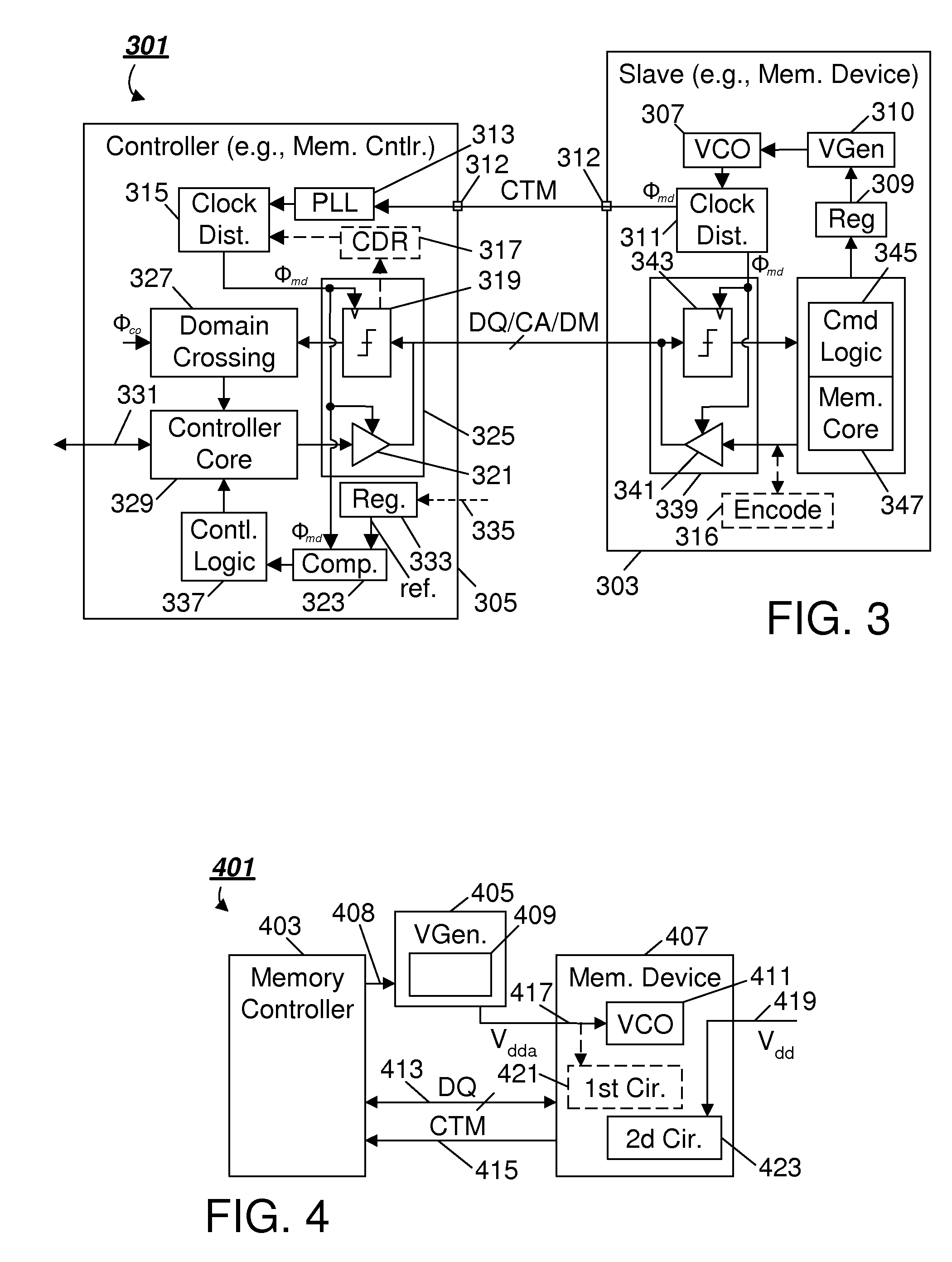
[0038]FIG. 4 presents a variant on the basic design of the system just discussed; in particular, FIG. 4 presents an embodiment 401 having a memory controller 403, an external chip 405 (used for purposes of adjusting memory timing) and a memory device 407. In this particular example, the memory controller uses a dedicated link 408 to control the adjustment of a VCO control voltage (Vdda) provided to the memory device, by programming a register or other storage element 409. That is, unlike previous embodiments, the register or other storage element in FIG. 4 is located on an external chip, such as an external voltage regulator 405. As was the case with the previous discussion, each of these elements (memory controller 403, external chip 405 and memory device 407) may be standalone integrated circuits, single die or otherwise. The VCO control (Vdda) applied by the memory device is used to vary memory device data rate and timing through control of VCO 411, with DQ links and a CTM signal...
PUM
 Abstract
Description
Claims
Application Information


