Small form-factor pluggable optical transceiver
a technology of plugging and optical transceivers, applied in the field of optoelectronic communication and devices, can solve the problems of inability to eliminate overheating of optical devices, relatively low efficiency, and inability to overheat optical devices, so as to improve yield, increase thermal issues, and increase port densities
- Summary
- Abstract
- Description
- Claims
- Application Information
AI Technical Summary
Benefits of technology
Problems solved by technology
Method used
Image
Examples
embodiment 1
[0028
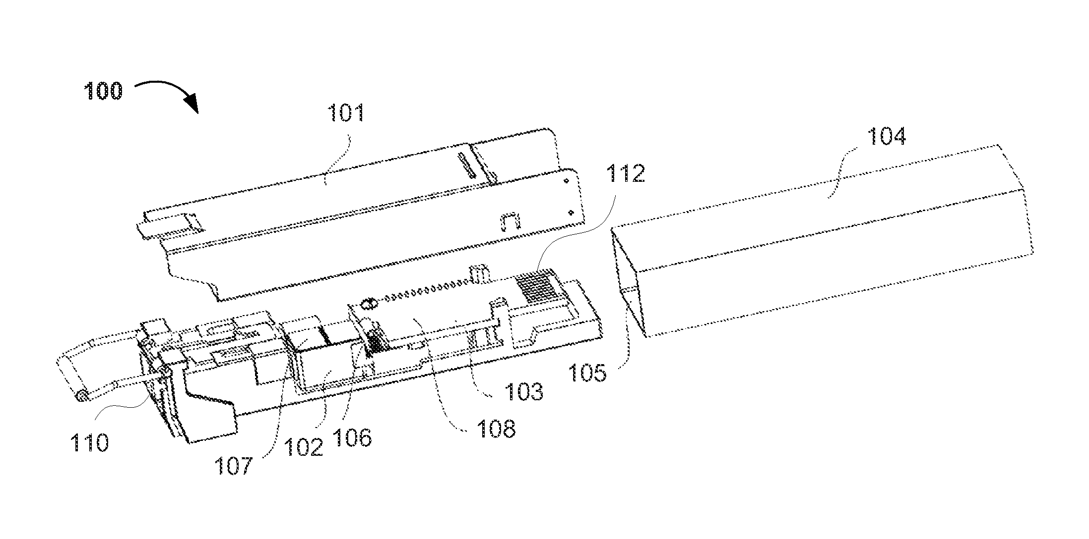
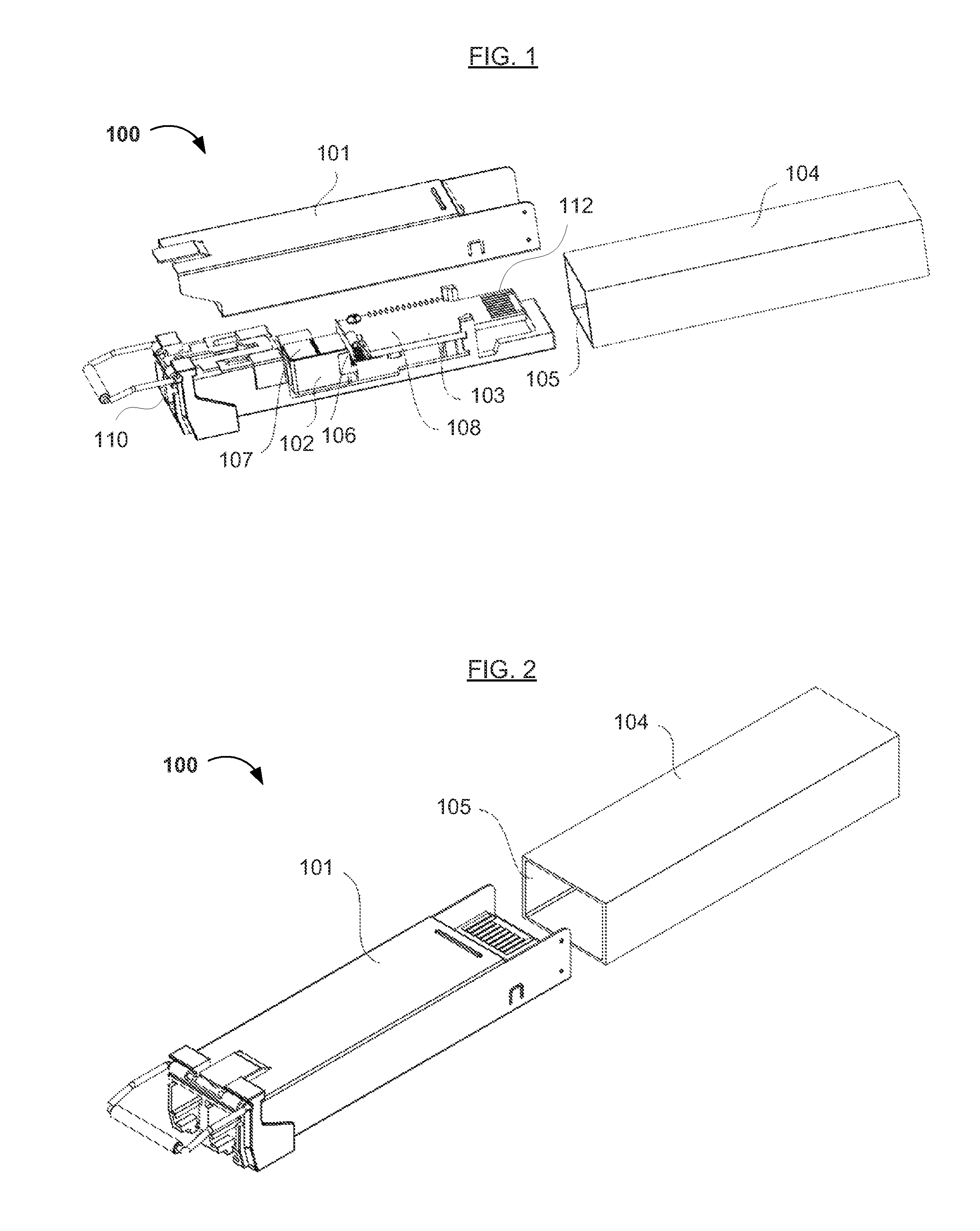
[0029]As shown in FIG. 1, a small form-factor pluggable (SFP) optical transceiver 100 comprises a casing 101 having an optical port 110 and an electrical port 112. The casing 101 is configured to accommodate optical devices 102 and electrical devices 103. The optical device 102 comprises a transceiver optical subassembly (TOSA) and a receiver optical subassembly (ROSA). The electrical devices 103 are located on a printed circuit board (PCB) on or near the bottom of the casing 101.
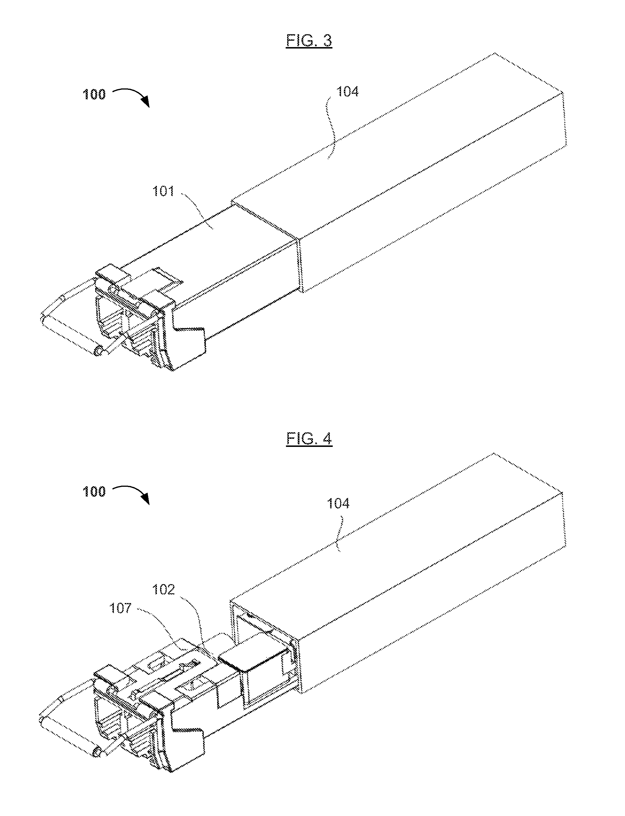
[0030]As shown in FIGS. 2-4, during normal operation, the casing 101 is connected to a switchboard 104 via a connector 105 located in the switchboard 104. As shown more clearly in FIG. 3, one portion of the casing 101 stays outside of the switchboard 104 after the casing 101 is inserted into the connector 105 located in the switchboard 104. More specifically, the electrical devices 103 inside the casing 101 and the portion of the casing 101 enclosing the electrical devices 103 stay inside the switchboa...
embodiment 2
[0032
[0033]As shown in FIGS. 5 and 6, based on or from Embodiment 1 above, an SFP optical transceiver 200 (or a casing 201 therefor) has a built-in (e.g., internal) isolator 206. The isolator 206 is configured to divide the transceiver 200 (or casing 201) into a first cavity 207 close to or facing the optical port 210 and a second cavity 208 close to or facing the electrical port 212. The optical devices (not shown) are located in the first cavity 207, and the electrical devices (not shown) are located in the second cavity 208. After the transceiver 200 (or casing 201) is divided into two relatively independent cavities via the isolator 206, the portion 208 containing the electrical devices having a relatively high temperature is isolated from the portion 207 containing the optical devices. Heat produced by the electrical device portion 203 having a high temperature during normal operation can be blocked from being transferred to the cavity 207 where the optical devices are located,...
embodiment 3
[0038
[0039]Referring back to FIGS. 1 and 4, Embodiment 3 is different from directly setting the isolator 106 inside the casing 101, as described in Embodiment 2 above. In this embodiment (e.g., Embodiment 3), the isolator 106 and the casing 101 may be connected by a latching mechanism. More specifically, a bottom surface (e.g., face) of the casing 101 may have a tapered end, and the isolator 106 may have a groove compatible with the tapered end. The connection between the isolator 106 and the casing 101 is implemented by the tapered end effectively working or mating with the groove. Consequently, the optical device portion 102 may be easily removed or dismounted, and the connection between the optical devices 102 and the electrical devices 103 may be enhanced.
[0040]The other structures of this embodiment (e.g., Embodiment 3) have been explained in greater detail with respect to Embodiments 1 and 2.
PUM
 Abstract
Description
Claims
Application Information


